MCP1826-3302E/AT Microchip Technology, MCP1826-3302E/AT Datasheet - Page 18
MCP1826-3302E/AT
Manufacturer Part Number
MCP1826-3302E/AT
Description
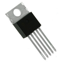
IC LDO REG 1A 3.3V TO220-5
Manufacturer
Microchip Technology
Datasheet
1.MCP1826T-1202EDC.pdf
(36 pages)
Specifications of MCP1826-3302E/AT
Regulator Topology
Positive Fixed
Voltage - Output
3.3V
Voltage - Input
Up to 6V
Voltage - Dropout (typical)
0.25V @ 1A
Number Of Regulators
1
Current - Output
1A (Min)
Operating Temperature
-40°C ~ 125°C
Mounting Type
Through Hole
Package / Case
TO-220-5 (Straight Leads)
Primary Input Voltage
3.7V
Output Voltage
3.3V
Dropout Voltage Vdo
250mV
No. Of Pins
5
Output Current
1A
Voltage Regulator Case Style
TO-220
Operating Temperature Range
-40°C To +125°C
Svhc
No SVHC
Output Voltage Fixed
3.3V
Rohs Compliant
Yes
Number Of Outputs
1
Polarity
Positive
Input Voltage Max
6 V
Output Type
Fixed
Dropout Voltage (max)
0.4 V at 1 A
Line Regulation
0.05 % / V
Load Regulation
0.5 %
Voltage Regulation Accuracy
2 %
Maximum Operating Temperature
+ 125 C
Mounting Style
Through Hole
Minimum Operating Temperature
- 40 C
Lead Free Status / RoHS Status
Lead free / RoHS Compliant
Current - Limit (min)
-
Lead Free Status / Rohs Status
Details


MCP1826/MCP1826S
the 30 µs delay, the LDO output enters its soft-start
period as it rises from 0V to its final regulation value. If
the SHDN input signal is pulled low during the 30 µs
delay period, the timer will be reset and the delay time
will start over again on the next rising edge of the
SHDN input. The total time from the SHDN input going
high (turn-on) to the LDO output being in regulation is
typically 100 µs. See
the SHDN input.
FIGURE 4-4:
Diagram.
DS22057A-page 18
V
SHDN
OUT
30 µs
T
OR
70 µs
Figure 4-4
Shutdown Input Timing
for a timing diagram of
400 ns (typ)
4.7
Dropout voltage is defined as the input-to-output
voltage differential at which the output voltage drops
2% below the nominal value that was measured with a
V
MCP1826S LDO has a very low dropout voltage
specification of 300 mV (typical) at 1000 mA of output
current. See Section 1.0 “Electrical Characteristics”
for maximum dropout voltage specifications.
The MCP1826/MCP1826S LDO operates across an
input voltage range of 2.3V to 6.0V and incorporates
input Undervoltage Lockout (UVLO) circuitry that keeps
the LDO output voltage off until the input voltage
reaches a minimum of 2.00V (typical) on the rising
edge of the input voltage. As the input voltage falls, the
LDO output will remain on until the input voltage level
reaches 1.82V (typical).
Since the MCP1826/MCP1826S LDO undervoltage
lockout activates at 1.82V as the input voltage is falling,
the dropout voltage specification does not apply for
output voltages that are less than 1.8V.
For high-current applications, voltage drops across the
PCB traces must be taken into account. The trace
resistances can cause significant voltage drops
between the input voltage source and the LDO. For
applications with input voltages near 2.3V, these PCB
trace voltage drops can sometimes lower the input
voltage enough to trigger a shutdown due to
undervoltage lockout.
4.8
The MCP1826/MCP1826S LDO has temperature-
sensing circuitry to prevent the junction temperature
from exceeding approximately 150
junction temperature does reach 150
output will be turned off until the junction temperature
cools to approximately 140
output will automatically resume normal operation. If
the internal power dissipation continues to be
excessive, the device will again shut off. The junction
temperature of the die is a function of power dissipa-
tion, ambient temperature and package thermal
resistance. See Section 5.0 “Application Circuits/
Issues” for more information on LDO power
dissipation and junction temperature.
R
+ 0.5V differential applied. The MCP1826/
Dropout Voltage and Undervoltage
Lockout
Overtemperature Protection
© 2007 Microchip Technology Inc.
°
C, at which point the LDO
°
C. If the LDO
°
C, the LDO
Related parts for MCP1826-3302E/AT
Image
Part Number
Description
Manufacturer
Datasheet
Request
R

Part Number:
Description:
1A CMOS LDO, Vout=3.0V, Extended Temp Range 5 TO-220 TUBE
Manufacturer:
Microchip Technology
Datasheet:

Part Number:
Description:
1A CMOS LDO, Vout=3.0V, Extended Temp Range 5 DDPAK TUBE
Manufacturer:
Microchip Technology
Datasheet:
Part Number:
Description:
1A CMOS LDO, Adjustable Vout, Extended Temp Range 5 DDPAK TUBE
Manufacturer:
Microchip Technology
Datasheet:
Part Number:
Description:
IC LDO REG 1A 1.8V TO220-5
Manufacturer:
Microchip Technology
Datasheet:
Part Number:
Description:
IC LDO REG 1A 2.5V TO220-5
Manufacturer:
Microchip Technology
Datasheet:
Part Number:
Description:
IC LDO REG 1A 1.2V TO220-5
Manufacturer:
Microchip Technology
Datasheet:
Part Number:
Description:
IC LDO REG 1A 5.0V TO220-5
Manufacturer:
Microchip Technology
Datasheet:
Part Number:
Description:
IC LDO REG 1A ADJ-V TO220-5
Manufacturer:
Microchip Technology
Datasheet:
Part Number:
Description:
1A CMOS LDO, Vout=0.8V, Extended Temp Range 5 TO-220 TUBE
Manufacturer:
Microchip Technology
Datasheet:
Part Number:
Description:
1A CMOS LDO, Vout=0.8V, Extended Temp Range 5 DDPAK TUBE
Manufacturer:
Microchip Technology
Datasheet:
Part Number:
Description:
1A CMOS LDO, Vout=1.2V, Extended Temp Range 5 DDPAK TUBE
Manufacturer:
Microchip Technology
Datasheet:
Part Number:
Description:
1A CMOS LDO, Vout=1.8V, Extended Temp Range 5 DDPAK TUBE
Manufacturer:
Microchip Technology
Datasheet:
Part Number:
Description:
1A CMOS LDO, Vout=2.5V, Extended Temp Range 5 DDPAK TUBE
Manufacturer:
Microchip Technology
Datasheet:
Part Number:
Description:
1A CMOS LDO, Vout=3.3V, Extended Temp Range 5 DDPAK TUBE
Manufacturer:
Microchip Technology
Datasheet:
Part Number:
Description:
1A CMOS LDO, Vout=5.0V, Extended Temp Range 5 DDPAK TUBE
Manufacturer:
Microchip Technology
Datasheet: