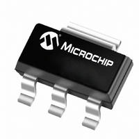
TC1262-3.0VDB Microchip Technology, TC1262-3.0VDB Datasheet - Page 4

TC1262-3.0VDB
Manufacturer Part Number
TC1262-3.0VDB
Description
IC CMOS LDO 500MA 3.0V SOT-223
Manufacturer
Microchip Technology
Datasheet
1.TC1262-3.3VDBTR.pdf
(12 pages)
Specifications of TC1262-3.0VDB
Package / Case
SOT-223 (3 leads + Tab), SC-73, TO-261
Regulator Topology
Positive Fixed
Voltage - Output
3V
Voltage - Input
Up to 6V
Voltage - Dropout (typical)
0.35V @ 500mA
Number Of Regulators
1
Current - Output
500mA (Min)
Operating Temperature
-40°C ~ 125°C
Mounting Type
Surface Mount
Number Of Outputs
1
Input Voltage Max
6 V
Output Voltage
3 V
Output Voltage Tolerance
2 %
Output Type
Fixed
Dropout Voltage (max)
650 mV
Output Current
500 mA
Line Regulation
0.003 V
Load Regulation
0.002 mA
Voltage Regulation Accuracy
0.5 %
Maximum Operating Temperature
+ 125 C
Mounting Style
SMD/SMT
Minimum Operating Temperature
- 40 C
Lead Free Status / RoHS Status
Lead free / RoHS Compliant
Current - Limit (min)
-
Lead Free Status / Rohs Status
Lead free / RoHS Compliant
Available stocks
Company
Part Number
Manufacturer
Quantity
Price
Company:
Part Number:
TC1262-3.0VDB
Manufacturer:
MICROCHIP
Quantity:
12 000
Part Number:
TC1262-3.0VDB
Manufacturer:
MICROCHIP/微芯
Quantity:
20 000
TC1262
4.0
4.1
Integrated thermal protection circuitry shuts the
regulator off when die temperature exceeds 160°C.
The regulator remains off until the die temperature
drops to approximately 150°C.
4.2
The amount of power the regulator dissipates is
primarily a function of input and output voltage, and
output current. The following equation is used to
calculate worst case actual power dissipation:
EQUATION 4-1:
The maximum allowable power dissipation (Equation
4-2) is a function of the maximum ambient temperature
(T
(T
(θ
EQUATION 4-2:
Table 4-1 and Table 4-2 show various values of θ
the TC1262 packages.
TABLE 4-1:
*Tab of device attached to topside copper
DS21373B-page 4
2500 sq mm 2500 sq mm 2500 sq mm
1000 sq mm 2500 sq mm 2500 sq mm
1000 sq mm 1000 sq mm 1000 sq mm
1000 sq mm
225 sq mm
100 sq mm
(Topside)*
A
JA
J
MAX
MAX
Copper
I
).
Where:
LOAD
V
Area
V
OUT
) and the thermal resistance from junction-to-air
), the maximum allowable die temperature
IN
Where all terms are previously defined.
MAX
MAX
THERMAL CONSIDERATIONS
Thermal Shutdown
Power Dissipation
P
MIN
D
P
= Worst case actual power dissipation
= Maximum voltage on V
= Minimum regulator output voltage
= Maximum output (load) current
D
2500 sq mm 2500 sq mm
2500 sq mm 2500 sq mm
(Backside)
≈ (V
P
0 sq mm
Copper
D
THERMAL RESISTANCE
GUIDELINES FOR TC1262 IN
SOT-223 PACKAGE
Area
MAX
IN
MAX
= (T
– V
J
MAX
OUT
θ
1000 sq mm
JA
– T
Board
Area
MIN
A
)I
MAX
LOAD
IN
)
MAX
Resistance
Thermal
45°C/W
45°C/W
53°C/W
59°C/W
52°C/W
55°C/W
(θ
JA
JA
)
for
TABLE 4-2:
*Tab of device attached to topside copper
Equation 4-1 can be used in conjunction with Equation
4-2 to ensure regulator thermal operation is within
limits. For example:
Given:
Find: 1. Actual power dissipation
Actual power dissipation:
P
Maximum allowable power dissipation:
In this example, the TC1262 dissipates a maximum of
260mW; below the allowable limit of 508mW. In a
similar manner, Equation 4-1 and Equation 4-2 can be
used to calculate maximum current and/or input
voltage limits. For example, the maximum allowable
V
power dissipation of 508mW into Equation 4-1, from
which V
2500 sq mm 2500 sq mm 2500 sq mm
1000 sq mm 2500 sq mm 2500 sq mm
D
IN
125 sq mm
(Topside)*
Copper
, is found by sustituting the maximum allowable
≈ (V
= [(3.3 x 1.1) – (2.7 x .995)]275 x 10
= 260mW
P
Area
V
V
I
T
T
θ
D
LOAD
A
JA
J
IN
OUT
2. Maximum allowable dissipation
MAX
MAX
MAX
IN
MAX
IN
MAX
MAX
MIN
= (125 – 95)
= 508mW
= (T
MAX
– V
= 4.6V.
J
= 3.3V ± 10%
= 2.7V ± 0.5%
= 275mA
= 125°C
= 95°C
= 59°C/W (SOT-223)
2500 sq mm 2500 sq mm
MAX
(Backside)
59
OUT
Copper
θ
THERMAL RESISTANCE
GUIDELINES FOR TC1262 IN
3-PIN DDPAK/TO-220
PACKAGE
Area
– T
JA
MIN
A
)I
MAX
©
LOAD
2002 Microchip Technology Inc.
)
MAX
Board
Area
–3
Resistance
Thermal
25°C/W
27°C/W
35°C/W
(θ
JA
)


