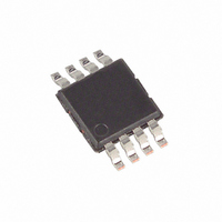
MAX1806EUA33+ Maxim Integrated Products, MAX1806EUA33+ Datasheet - Page 7

MAX1806EUA33+
Manufacturer Part Number
MAX1806EUA33+
Description
IC REG 3.3V/ADJ 500MA 8-UMAX
Manufacturer
Maxim Integrated Products
Datasheet
1.MAX1806EUA33.pdf
(10 pages)
Specifications of MAX1806EUA33+
Regulator Topology
Positive Fixed or Adjustable
Voltage - Output
3.3V, 0.8 ~ 4.5 V
Voltage - Input
2.25 ~ 5.5 V
Number Of Regulators
1
Current - Output
500mA (Min)
Operating Temperature
-40°C ~ 85°C
Mounting Type
Surface Mount
Package / Case
8-MSOP, Micro8™, 8-uMAX, 8-uSOP,
Number Of Outputs
1
Polarity
Positive
Input Voltage Max
5.5 V
Output Voltage
3.3 V
Output Type
Adjustable, Fixed
Dropout Voltage (max)
315 mV
Output Current
500 mA
Line Regulation
0.125 %/V
Load Regulation
15.5 ppm/mA
Voltage Regulation Accuracy
1 %
Maximum Power Dissipation
1.3 W
Maximum Operating Temperature
+ 85 C
Mounting Style
SMD/SMT
Minimum Operating Temperature
- 40 C
Reference Voltage
0.8 V
Lead Free Status / RoHS Status
Lead free / RoHS Compliant
Voltage - Dropout (typical)
-
Current - Limit (min)
-
Lead Free Status / Rohs Status
Lead free / RoHS Compliant
The MAX1806 is a low-dropout, low-quiescent-current
linear regulator. The device supplies loads up to
500mA and is available with preset output voltages. As
illustrated in Figure 1, the MAX1806 includes a 0.8V ref-
erence, error amplifier, P-channel pass transistor, and
internal feedback voltage-divider.
The reference is connected to the error amplifier, which
compares it with the feedback voltage and amplifies
the difference. If the feedback voltage is lower than the
reference voltage, the pass-transistor gate is pulled
lower, which allows more current to pass to the output
increasing the output voltage. If the feedback voltage is
too high, the pass-transistor gate is pulled up, allowing
less current to pass to the output.
The output voltage is fed back through either an inter-
nal resistive voltage-divider connected to OUT or an
external resistor network connected to SET. The dual-
mode comparator examines V
back path. If V
path is used, and the output is regulated to the factory-
preset voltage. Additional blocks include an output cur-
rent limiter, thermal sensor, and shutdown logic.
The MAX1806 features a 0.4Ω P-channel MOSFET pass
transistor. Unlike similar designs using PNP pass tran-
sistors, P-channel MOSFETs require no base drive,
which reduces operating current. PNP-based regula-
tors also waste considerable current in dropout when
the pass transistor saturates, and use high base-drive
currents under large loads. The MAX1806 does not suf-
fer from these problems.
The MAX1806’s dual-mode operation allows operation
in either a preset voltage mode or an adjustable mode.
Connect SET to GND to select the preset output volt-
age. The two-digit part number suffix identifies the out-
put voltage (see Selector Guide). For example, the
MAX1806EUA33 has a preset 3.3V output voltage. The
output voltage may also be adjusted by connecting a
voltage-divider from OUT to SET (Figure 2). Select R2 in
the 25kΩ to 100kΩ range. Calculate R1 with the follow-
ing equation:
where V
to 4.5V.
Drive SHDN low to enter shutdown. During shutdown,
the output is disconnected from the input, and supply
500mA, Low-Voltage Linear Regulator in µMAX
SET
Internal P-Channel Pass Transistor
= 0.8V, and V
R1 = R2 [(V
SET
_______________________________________________________________________________________
is below 35mV, the internal feedback
Detailed Description
Output Voltage Selection
OUT
OUT
SET
/ V
SET
may range from 0.8V
and selects the feed-
) - 1]
Shutdown
current drops to 0.02µA. When in shutdown, POK pulls
low. The capacitance and load at OUT determine the
rate at which V
high as +6V, regardless of the input and output voltage.
The POK output pulls low when OUT is less than 93% of
the nominal regulation voltage. Once OUT exceeds
93% of the nominal voltage, POK goes high imped-
ance. POK is an open-drain N-channel output. To
obtain a logic voltage output, connect a pullup resistor
from POK to OUT. A 100kΩ resistor works well for most
applications. POK can be used to signal a microcon-
troller (µC), or drive an external LED to indicate power
failure. When the MAX1806 is shutdown, POK is held
low independent of the output voltage. If unused, leave
POK grounded or unconnected.
The MAX1806 monitors and controls the pass transis-
tor’s gate voltage, limiting the output current to 1.4A
(typ). The output can be shorted to ground for an indefi-
nite period of time without damaging the part.
Thermal overload protection limits total power dissipa-
tion in the MAX1806. When the junction temperature
exceeds T
pass transistor, allowing the device to cool. The thermal
sensor turns the pass transistor on again after the junc-
tion temperature cools by 20°C, resulting in a pulsed
output during continuous thermal overload conditions.
Thermal overload protection protects the MAX1806 in
the event of fault conditions. For continuous operation,
do not exceed the absolute maximum junction-temper-
ature rating of T
The MAX1806’s maximum power dissipation depends
on the thermal resistance of the IC package and circuit
board, the temperature difference between the die
junction and ambient air, and the rate of air flow. The
power dissipated in the device is P = I
V
1.3W or:
where T
MAX1806 die junction and the surrounding air, θ
the thermal resistance from the junction to the case,
and θ
through the PC board, copper traces, and other materi-
als to the surrounding air. The MAX1806 package fea-
tures an exposed thermal pad on its underside. This
pad lowers the package’s thermal resistance by provid-
OUT
Operating Region and Power Dissipation
). The maximum allowed power dissipation is
CA
J
PMAX = (T
- T
is the thermal resistance from the case
J
A
= +170°C, a thermal sensor turns off the
is the temperature difference between the
J
OUT
= +150°C.
Thermal Overload Protection
decays. SHDN can be pulled as
J(MAX)
- T
A
) / (θ
Power-OK Output
JC
Current Limit
+ θ
OUT
CA
)
✕
(V
JC
IN
is
7
-


