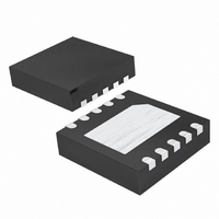
MAX15027ATB+T Maxim Integrated Products, MAX15027ATB+T Datasheet - Page 9

MAX15027ATB+T
Manufacturer Part Number
MAX15027ATB+T
Description
IC LDO REG ADJ 1A 10-TDFN
Manufacturer
Maxim Integrated Products
Datasheet
1.MAX15028ATBT.pdf
(11 pages)
Specifications of MAX15027ATB+T
Regulator Topology
Positive Adjustable
Voltage - Output
0.5 ~ 3.3 V
Voltage - Input
1.43 ~ 3.6 V
Voltage - Dropout (typical)
0.075V @ 1A
Number Of Regulators
1
Current - Output
1A
Current - Limit (min)
1.4A
Operating Temperature
-40°C ~ 125°C
Mounting Type
Surface Mount
Package / Case
10-TDFN Exposed Pad
Lead Free Status / RoHS Status
Lead free / RoHS Compliant
Other names
MAX15027ATB+T
MAX15027ATB+TTR
MAX15027ATB+TTR
Capacitors are required at the MAX15027/MAX15028’s
inputs and outputs for stable operation over the full
temperature range and with load currents up to 1A.
Connect a 1µF capacitor between IN and ground and a
4.7µF capacitor with low equivalent series resistance
(ESR) between OUT and ground for 1A output current.
The input capacitor (C
of the input supply. If input supply source impedance is
high, place a larger input capacitor close to IN to pre-
vent V
capacitors can be used for output currents less than
1A. Calculate the minimum C
The maximum power dissipation depends on the ther-
mal resistance of the IC package and circuit board, the
temperature difference between the die junction and
ambient air, and the rate of airflow. The power dissipat-
ed in the device is P
package features an exposed thermal pad on its
underside. This pad lowers the thermal resistance of
the package by providing a direct heat conduction
path from the die to the PCB. Connect the exposed
backside pad and GND to the system ground using a
large pad or ground plane and multiple vias to the
ground plane layer.
IN
sagging due to load transients. Smaller output
C
OUT
_______________________________________________________________________________________
=
I
OUT MAX
IN
DISS
Capacitor Selection and
) lowers the source impedance
1.425V to 3.6V Input, 1A Low-Dropout
(
Operating Region and
= I
OUT
)
Regulator Stability
OUT
×
Power Dissipation
as follows:
⎛
⎜
⎝
0 25
1
.
(V
µ
F
IN
A
⎞
⎟
⎠
- V
OUT
). The
Regulators with BIAS Input
The MAX15027/MAX15028 are designed to operate
with low-dropout voltages and low quiescent currents
while still maintaining good noise performance, tran-
sient response, and AC rejection (see the Typical
Operating Characteristics for a plot of Power-Supply
Rejection Ratio (PSRR) vs. Frequency). When operating
from noisy sources, improved supply-noise rejection
and transient response can be achieved by increasing
the values of the input and output bypass capacitors
and through passive filtering techniques. The
MAX15027/MAX15028 load-transient response graphs
(see the Typical Operating Characteristic s) show two
components of the output response: a DC shift from the
output impedance due to the load current change, and
the transient response. A typical transient overshoot for
a step change in the load current from 300mA to
800mA is 15mV. Use ceramic output capacitors greater
than 4.7µF (up to 100µF) to attenuate the overshoot.
The TDFN package has an exposed thermal pad on its
underside. This pad provides a low thermal resistance
path for heat transfer into the PCB. This low thermally
resistive path carries a majority of the heat away from
the IC. The PCB is effectively a heatsink for the IC. The
exposed pad should be connected to a large ground
plane for proper thermal and electrical performance.
The minimum size of the ground plane is dependent
upon many system variables. To create an efficient
path, the exposed pad should be soldered to a thermal
landing, which is connected to the ground plane by
thermal vias. The thermal landing should be at least as
large as the exposed pad.
Noise, PSRR, and Transient Response
Layout Guidelines
9


