NCP584LSN18T1G ON Semiconductor, NCP584LSN18T1G Datasheet
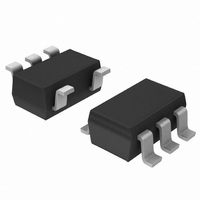
IC REG LDO 200MA 1.8V SOT23-5

NCP584LSN18T1G

Manufacturer Part Number
NCP584LSN18T1G
Description
IC REG LDO 200MA 1.8V SOT23-5
Manufacturer
ON Semiconductor
Datasheet

Specifications of NCP584LSN18T1G

Regulator Topology
Positive Fixed
Voltage - Output
1.8V
Voltage - Input
Up to 6V
Voltage - Dropout (typical)
0.2V @ 200mA
Number Of Regulators
1
Current - Output
200mA (Min)
Operating Temperature
-40°C ~ 85°C
Mounting Type
Surface Mount
Package / Case
SOT-23-5, SC-74A, SOT-25
Number Of Outputs
1
Polarity
Positive
Input Voltage Max
6 V
Output Voltage
1.8 V
Output Type
Fixed
Dropout Voltage (max)
0.3 V at 200 mA
Output Current
200 mA
Line Regulation
0.3 % / V
Load Regulation
40 mV
Voltage Regulation Accuracy
3 %
Maximum Power Dissipation
0.25 W
Maximum Operating Temperature
+ 85 C
Mounting Style
SMD/SMT
Minimum Operating Temperature
- 40 C
Lead Free Status / RoHS Status
Lead free / RoHS Compliant
Current - Limit (min)
-
Lead Free Status / Rohs Status
 Details
Other names
NCP584LSN18T1GOSTR

Available stocks

Company
Part Number
Manufacturer
Quantity
Price
Part Number:
NCP584LSN18T1G
Manufacturer:
ON Semiconductor
Quantity:
1 750
Part Number:
NCP584LSN18T1G
Manufacturer:
ON/安森美
Quantity:
20 000
Company:
Part Number:
NCP584LSN18T1G
Quantity:
120
NCP584
Tri-Mode 200 mA CMOS
LDO Regulator with Enable
portable battery powered applications which require precise output
voltage accuracy, low quiescent current, and high ripple rejection.
These devices feature an enable function which lowers current
consumption significantly and are offered in the SOT23−5 package.
Fast Transient Mode (FT mode), and Low Power Mode (LP mode).
Both the FT and LP mode are utilized via the ECO pin.
Features
Typical Applications
© Semiconductor Components Industries, LLC, 2010
February, 2010 − Rev. 14
CE
V
The NCP584 series of low drop out regulators are designed for
This series of devices have three modes. Chip Enable (CE mode),
in
"100 ppm/°C
Tri−mode Operation
Low Dropout Voltage of 400 mV at 200 mA, Output Voltage = 0.9 V
Excellent Line Regulation of 0.05%/V (0.10% LP Mode)
Excellent Load Regulation of 10 mV (20 mV FT Mode)
High Output Voltage Accuracy of ±2% (±3% LP mode)
Ultra−Low Iq Current of:
Very Low Shutdown Current of 0.1 mA
Excellent Power Supply Rejection Ratio of 75 dB at f = 1.0 kHz
Low Temperature Drift Coefficient on the Output Voltage of
Fold Back Protection Circuit
Input Voltage up to 6.5 V
These are Pb−Free Devices
Portable Equipment
Hand−Held Instrumentation
Camcorders and Cameras
Figure 1. Simplified Block Diagram for Active Low
3.5 mA (LP mode, Output Voltage ≤ 1.5 V)
40 mA (FT mode)
V
ref
Current Limit
+
-
300 mV at 200 mA, Output Voltage = 1.2 V
200 mV at 200 mA, Output Voltage = 1.8 V
ECO
V
GND
out
1
CE
V
in
Figure 2. Simplified Block Diagram for Active High
See detailed ordering and shipping information in the package
dimensions section on page 13 of this data sheet.
*Additional voltage options may be available between
0.8 V and 3.3 V in 100 mV steps.
V
ref
1
Current Limit
ORDERING INFORMATION
+
-
5
XXX = Specific Device Code
TT
http://onsemi.com
= Traceability Information
SN SUFFIX
CASE 1212
SOT23−5
Publication Order Number:
ECO
5
1
MARKING
DIAGRAM
XXXTT
NCP584/D
V
GND
out

Related parts for NCP584LSN18T1G

NCP584LSN18T1G Summary of contents

Page 1

NCP584 Tri-Mode 200 mA CMOS LDO Regulator with Enable The NCP584 series of low drop out regulators are designed for portable battery powered applications which require precise output voltage accuracy, low quiescent current, and high ripple rejection. These devices feature ...

Page 2

PIN FUNCTION DESCRIPTION SOT23−5 Pin Name GND ECO 5 V out MAXIMUM RATINGS Rating Input Voltage Input Voltage ( Pin) Input Voltage (ECO Pin) Output Voltage Output Current Power ...

Page 3

ELECTRICAL CHARACTERISTICS (V Characteristic Input Voltage Output Voltage (1.0 mA ≤ I ≤ 30 mA) out ECO GND ECO Line Regulation ( mA 0.5 V ≤ V out out FT ...

Page 4

nominal +2 out 0 nominal + V (max) in out DO 0.5 0.4 0.3 V out 0.2 ECO = H 0.1 0 100 200 OUTPUT CURRENT I out ...

Page 5

INPUT VOLTAGE V in Figure 9. Quiescent Current vs. Input Voltage 4.3 0.3 1.3 2.3 3.3 INPUT VOLTAGE V ...

Page 6

TEMPERATURE (°C) Figure 15. Output Voltage vs. Temperature 0.6 0.5 25°C 0.4 0.3 0.2 0.1 0 100 125 OUTPUT CURRENT I out Figure 17. ...

Page 7

OUTPUT CURRENT I out Figure 21. Dropout Voltage vs. Output Current 90 I out 1.0 mA out ...

Page 8

Input Voltage ECO = out ms 1 out nominal out out Output Voltage TIME, ...

Page 9

Load Current ECO = nominal + 1 out C = 1 out nominal out out Output Voltage − ...

Page 10

1 1.8 ECO = 1.0 mF 2.2 mF out 0.6 0.0 I out TIME, t (ms) Figure 29. Turn−On/Off Speed ...

Page 11

V − 1.3 V 0.94 ECO 0.93 0. 0.91 out 0.90 0. 0.91 out 0.90 0. 0.91 out 0.90 0. out ...

Page 12

Input Decoupling A 1.0 mF tantalum capacitor is the recommended value to be connected between V and GND. For PCB layout in considerations, the traces of V and GND should be in sufficiently wide in order to minimize noise and ...

Page 13

... Active Low, LP and FT Mode NCP584LSN12T1G Active Low, LP and FT Mode NCP584LSN18T1G Active Low, LP and FT Mode †For information on tape and reel specifications, including part orientation and tape sizes, please refer to our Tape and Reel Packaging Specification Brochure, BRD8011/D. Other voltages are available. Consult your ON Semiconductor representative. ...

Page 14

... SCALE 10:1 *For additional information on our Pb−Free strategy and soldering details, please download the ON Semiconductor Soldering and Mounting Techniques Reference Manual, SOLDERRM/D. N. American Technical Support: 800−282−9855 Toll Free USA/Canada Europe, Middle East and Africa Technical Support: ...

Related keywords