LP3876ES-ADJ/NOPB National Semiconductor, LP3876ES-ADJ/NOPB Datasheet
LP3876ES-ADJ/NOPB
Specifications of LP3876ES-ADJ/NOPB
LP3876ES-ADJ


Related parts for LP3876ES-ADJ/NOPB


LP3876ES-ADJ/NOPB Summary of contents
Page 1
... Adjustable Output Voltage: The output voltage may be programmed via two external resistors. Typical Application Circuit *See Application Hints © 2006 National Semiconductor Corporation Features n Ultra low dropout voltage n Low ground pin current n Load regulation of 0.08% n 1µA quiescent current in shutdown mode ...
Page 2
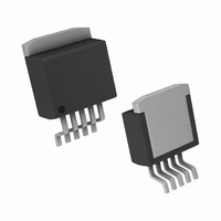
... LP3876-ADJ Name GND V OUT ADJ Current Description Package Type 3A TO263-5 LP3876ES-ADJ 3A TO263-5 LP3876ES-ADJ 3A TO220-5 LP3876ET-ADJ 2 20074406 Top View TO263-5 Package Function Shutdown Input Supply Ground Output Voltage Set Output Voltage 20074431 Package Marking Supplied As: Rail Tape and Reel Rail ...
Page 3
Block Diagram LP3876-ADJ 20074429 3 www.national.com ...
Page 4
... Absolute Maximum Ratings If Military/Aerospace specified devices are required, please contact the National Semiconductor Sales Office/ Distributors for availability and specifications. Storage Temperature Range Lead Temperature (Soldering, 5 sec.) ESD Rating (Note 3) Power Dissipation (Note 2) Input Supply Voltage (Survival) Shutdown Input Voltage (Survival) ...
Page 5
Electrical Characteristics LP3876-ADJ (Continued) Limits in standard typeface are for T J Unless otherwise specified O(NOM) Symbol Parameter SHUTDOWN INPUT V Shutdown Threshold SDT T Turn-off delay dOFF T Turn-on delay dON I SD Input Current ...
Page 6
Typical Performance Characteristics C = 10µF, S/D pin is tied Dropout Voltage Vs Output Load Current Ground Current vs Output Voltage IL=3A DC Load Reg. vs Junction Temperature www.national.com Unless otherwise specified ...
Page 7
Typical Performance Characteristics C = 10µF, S/D pin is tied OUT Over Temperature IN OUT Load Transient Response 10µF, OSCON IN OUT Load Transient Response C = ...
Page 8
Typical Performance Characteristics C = 10µF, S/D pin is tied Load Transient Response 100µF, TANTALUM IN OUT Load Transient Response 100µF, OSCON IN OUT Load Transient ...
Page 9
Application Hints SETTING THE OUTPUT VOLTAGE The output voltage is set using the resistors R1 and R2 (see Typical Application Circuit). The output is also dependent on the reference voltage (typically 1.216V) which is measured at the ADJ pin. The ...
Page 10
Application Hints (Continued) a severe temperature effect, losing more than 50% of nomi- nal capacitance at high and low limits of the temperature range. X7R and X5R dielectric ceramic capacitors are strongly rec- ommended if ceramics are used, as they ...
Page 11
Application Hints (Continued) the current drawn by the internal reference increases the total supply current (ground pin current). Using an optimized trade-off of ground pin current and die size, LP387X achieves low noise performance and low quiescent current operation. The ...
Page 12
Application Hints (Continued) FIGURE 2. Maximum power dissipation vs ambient temperature for TO-263 package www.national.com 20074433 12 ...
Page 13
Physical Dimensions inches (millimeters) unless otherwise noted TO220 5-lead, Molded, Stagger Bend Package (TO220-5) For Order Numbers, refer to the “Ordering Information” section of this document. TO263 5-Lead, Molded, Surface Mount Package (TO263-5) For Order Numbers, refer to the “Ordering ...
Page 14
... BANNED SUBSTANCE COMPLIANCE National Semiconductor follows the provisions of the Product Stewardship Guide for Customers (CSP-9-111C2) and Banned Substances and Materials of Interest Specification (CSP-9-111S2) for regulatory environmental compliance. Details may be found at: www.national.com/quality/green. ...