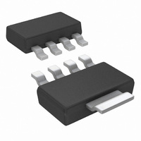
LP38693MP-ADJ/NOPB National Semiconductor, LP38693MP-ADJ/NOPB Datasheet

LP38693MP-ADJ/NOPB
Specifications of LP38693MP-ADJ/NOPB
LP38693MP-ADJTR
Related parts for LP38693MP-ADJ/NOPB
LP38693MP-ADJ/NOPB Summary of contents
Page 1
... Dropout Voltage: 250 mV (typ) @ 500mA (typ. 5V out). Ground Pin Current: 55 µA (typ) at full load. Adjust Pin Voltage: 2.0% (25°C) accuracy. Typical Application Circuits Note: *Minimum value required for stability. © 2011 National Semiconductor Corporation LP38691-ADJ LP38693-ADJ Features ■ LP38691QSD-ADJ is AEC-Q100 Grade 1 ■ ...
Page 2
... ADJ R1 and R2 (see Typical Application Circuit). LLP Only - The DAP (Exposed Pad) functions as a thermal connection when soldered to a copper DAP plane. See www.national.com 20126803 SOT-223, Top View LP38693MP-ADJ 20126804 Description LLP MOUNTING section in Application Hints 2 20126805 6-Lead LLP, Top View ...
Page 3
... Standard LP38691QSD-ADJ Automotive LP38691QSDX-ADJ Automotive LP38693MP-ADJ Standard LP38693MPX-ADJ Standard LP38693SD-ADJ Standard LP38693SDX-ADJ Standard Automotive Grade (Q) product incorporates enhanced manufacturing and support processes for the automotive market, including defect detection methodologies. Reliability qualification is compliant with the requirements and temperature grades defined in the AEC Q100 standard. Automotive Grade products are identified with the letter Q ...
Page 4
... Absolute Maximum Ratings If Military/Aerospace specified devices are required, please contact the National Semiconductor Sales Office/ Distributors for availability and specifications. Storage Temperature Range Lead Temp. (Soldering, 5 seconds) ESD Rating (Note 3) Power Dissipation (Note 2) V(max) All pins (with respect to GND) I OUT Junction Temperature Electrical Characteristics the full operating temperature range ...
Page 5
Symbol Parameter e Output Noise n V (LEAK) Output Leakage Current O V Enable Voltage (LP38693-ADJ EN Only) I Enable Pin Leakage (LP38693- EN ADJ Only) Note 1: Absolute maximum ratings indicate limits beyond which damage to the component may ...
Page 6
Block Diagrams FIGURE 2. LP38693-ADJ Functional Diagram (SOT-223, LLP) www.national.com FIGURE 1. LP38691-ADJ Functional Diagram (LLP) 6 20126806 20126807 ...
Page 7
Typical Performance Characteristics pin is tied to V (LP38693-ADJ only Noise vs Frequency Noise vs Frequency Ripple Rejection Unless otherwise specified 1.25V 2.7V 10mA 20126835 20126837 20126819 7 = ...
Page 8
V vs Temperature REF Line Transient Response Line Transient Response www.national.com Line Transient Response 20126830 Line Transient Response 20126824 Line Transient Response 20126826 8 20126823 20126825 20126827 ...
Page 9
Line Transient Response 20126828 Load Transient Response Load Regulation vs Temperature 20126854 Load Transient Response Enable Voltage vs Temperature 20126844 Line Regulation vs Temperature 9 20126842 20126853 20126855 www.national.com ...
Page 10
OUT IN OUT Power-Up OUT OFF (LP38693 Only) OUT EN www.national.com = 1.25V 20126858 20126860 20126862 1.80V OUT IN ...
Page 11
Dropout Voltage vs I OUT (V = 1.8V) OUT 20126857 11 www.national.com ...
Page 12
Application Hints EXTERNAL CAPACITORS Like any low-dropout regulator, external capacitors are re- quired to assure stability. These capacitors must be correctly selected for proper performance. INPUT CAPACITOR: An input capacitor of at least 1µF is re- quired (ceramic recommended). The ...
Page 13
If used in a dual-supply system where the regulator output load is returned to a negative supply, the output pin must be diode clamped to ground to limit the negative voltage transi- tion. A Schottky diode is recommended for this ...
Page 14
Physical Dimensions www.national.com inches (millimeters) unless otherwise noted 6-lead, LLP Package NS Package Number SDE06A SOT-223 Package NS Package Number MP05A 14 ...
Page 15
Notes 15 www.national.com ...
Page 16
... For more National Semiconductor product information and proven design tools, visit the following Web sites at: www.national.com Products Amplifiers www.national.com/amplifiers Audio www.national.com/audio Clock and Timing www.national.com/timing Data Converters www.national.com/adc Interface www.national.com/interface LVDS www.national.com/lvds Power Management www.national.com/power Switching Regulators www.national.com/switchers LDOs www.national.com/ldo LED Lighting www ...


