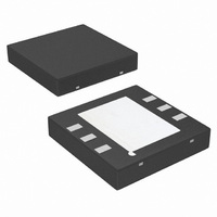
LP2992ILD-5.0/NOPB National Semiconductor, LP2992ILD-5.0/NOPB Datasheet - Page 5

LP2992ILD-5.0/NOPB
Manufacturer Part Number
LP2992ILD-5.0/NOPB
Description
IC REG LDO MICROPWR 250MA 6-LLP
Manufacturer
National Semiconductor
Datasheet
1.LP2992IM5-3.3NOPB.pdf
(16 pages)
Specifications of LP2992ILD-5.0/NOPB
Regulator Topology
Positive Fixed
Voltage - Output
5V
Voltage - Input
Up to 16V
Voltage - Dropout (typical)
0.45V @ 250mA
Number Of Regulators
1
Current - Output
250mA
Operating Temperature
-40°C ~ 125°C
Mounting Type
Surface Mount
Package / Case
6-LLP
Lead Free Status / RoHS Status
Lead free / RoHS Compliant
Current - Limit (min)
-
Other names
LP2992ILD-5.0
LP2992ILD-5.0TR
LP2992ILD-5.0TR
Available stocks
Company
Part Number
Manufacturer
Quantity
Price
Company:
Part Number:
LP2992ILD-5.0/NOPB
Manufacturer:
TRIQUINT
Quantity:
6 600
Part Number:
LP2992ILD-5.0/NOPB
Manufacturer:
TI/德州仪器
Quantity:
20 000
I
e
I
I
ON/OFF
O
O
n
(SC)
(PK)
Note 1: “Absolute Maximum Ratings” indicate limits beyond which damage to the component may occur. Electrical specifications do not apply when operating
the device outside of its rated operating conditions.
Note 2: The ESD rating of pins 3 and 4 for the SOT-23 package, or pins 1 and 3 for the LLP package, is 1 kV.
Note 3: The maximum allowable power dissipation is a function of the maximum junction temperature, T
A
Where the value of θ
dissipation will cause excessive die temperature, and the regulator will go into thermal shutdown.
Note 4: If used in a dual-supply system where the regulator load is returned to a negative supply, the LP2992 output must be diode-clamped to ground.
Note 5: The output PNP structure contains a diode between the V
will turn on this diode.
Note 6: Limits are 100% production tested at 25°C. Limits over the operating temperature range are guaranteed through correlation using Statistical Quality
Control (SQC) methods. The limits are used to calculate National's Average Outgoing Quality Level (AOQL).
Note 7: V
at which the output voltage drops 2% below the value measured with a 1V differential.
Note 8: The ON/OFF input must be properly driven to prevent possible misoperation. For details, refer to Application Hints.
Note 9: The LP2992 has foldback current limiting which allows a high peak current when V
forced to ground (see Typical Performance Characteristics curves).
, and the ambient temperature, T
Symbol
IN
must be the greater of 2.2V or V
ON/OFF Input Current
Output Noise
Voltage (RMS)
Ripple Rejection
Short Circuit Current
Peak Output Current
J-A
for the SOT-23 package is 220°C/W in a typical PC board mounting and the LLP package is 65°C/W. Exceeding the maximum allowable
Parameter
A
. The maximum allowable power dissipation at any ambient temperture is calculated using:
OUT(nom)
V
V
BW = 300 Hz to 50 kHz,
C
C
f = 1 kHz, C
C
R
(Note
V
ON/OFF
ON/OFF
OUT
OUT
BYPASS
OUT
L
+ Dropout Voltage to maintain output regulation. Dropout voltage is defined as the input to output differential
= 0 (Steady State)
≥
= 10 µF
= 10 µF
9)
V
= 0
= 5V
= 10 nF
Conditions
o
(NOM) −5%
BYPASS
IN
to V
OUT
= 10 nF
terminals that is normally reverse-biased. Reversing the polarity from V
5
OUT
0.01
Typ
400
350
30
45
5
> 0.5V, and then reduces the maximum output current as V
LP2992AI-X.X
Min
J
(MAX), the junction-to-ambient thermal resistance, θ
(Note
6)
Max
−2
15
Min
LP2992I-X.X
(Note
6)
Max
−2
15
www.national.com
IN
to V
Units
OUT
OUT
mA
mA
µA
µV
dB
J-
is


