LM317EMP/NOPB National Semiconductor, LM317EMP/NOPB Datasheet - Page 11
LM317EMP/NOPB
Manufacturer Part Number
LM317EMP/NOPB
Description
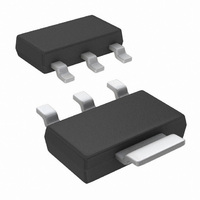
IC REG POSITIVE ADJ SOT-223
Manufacturer
National Semiconductor
Type
Voltage Regulatorr
Specifications of LM317EMP/NOPB
Regulator Topology
Positive Adjustable
Voltage - Output
1.2 ~ 37 V
Voltage - Input
4.2 ~ 40 V
Number Of Regulators
1
Current - Output
1A
Current - Limit (min)
1.5A
Operating Temperature
0°C ~ 125°C
Mounting Type
Surface Mount
Package / Case
SOT-223 (3 leads + Tab), SC-73, TO-261
Current, Output
1 A
Package Type
SOT-223
Regulation, Line
0.02 %/V
Regulation, Load
0.3 %
Regulator Type
Positive Voltage Out
Resistance, Thermal, Junction To Case
23.5 °C/W
Temperature, Operating, Range
0 to +125 °C
Voltage, Input
40 V
Voltage, Noise
0.003 %
Voltage, Output
1.2 to 37 V
Voltage, Supply, Rejection Ratio
80 dB
Lead Free Status / RoHS Status
Lead free / RoHS Compliant
Voltage - Dropout (typical)
-
Lead Free Status / Rohs Status
RoHS Compliant part
Electrostatic Device
Other names
LM317EMP
LM317EMPTR
LM317EMPTR
Available stocks
Company
Part Number
Manufacturer
Quantity
Price
Company:

Part Number:
LM317EMP/NOPB
Manufacturer:
NS
Quantity:
10 000
Part Number:
LM317EMP/NOPB
Manufacturer:
NS
Quantity:
20 000


HEATSINKING THE TO-263 PACKAGE
Figure 7
−A)
ounce copper and no solder mask over the copper area used
for heatsinking.
As shown in
square inch produces very little improvement. It should also
be observed that the minimum value of θ
package mounted to a PCB is 32°C/W.
FIGURE 6. Maximum Power Dissipation vs T
for different copper area sizes using a typical PCB with 1
FIGURE 5. θ
shows for the TO-263 the measured values of θ
Figure
(J−A)
7, increasing the copper area beyond 1
SOT-223 Package
SOT-223 Package
vs Copper (2 ounce) Area for the
(J−A)
for the TO-263
906357
906358
AMB
for the
(J
11
FIGURE 7. θ
As a design aid,
er dissipation compared to ambient temperature for the
TO-263 device (assuming θ
junction temperature is 125°C).
HEATSINKING THE TO-252 PACKAGE
If the maximum allowable value for θ
C/W (Typical Rated Value) for TO-252 package, no heatsink
is needed since the package alone will dissipate enough heat
to satisfy these requirements. If the calculated value for θ
falls below these limits, a heatsink is required.
As a design aid,
for different heatsink area. The copper patterns that we used
to measure these θ
Notes Section.
are in
Figure 10
vs. ambient temperature for the TO-252 device.
shows the maximum allowable power dissipation vs. copper
area (in
thermal enhancement techniques to be used with SOT-223
and TO-252 packages.
FIGURE 8. Maximum Power Dissipation vs T
Table
2
) for the TO-252 device. Please see AN-1028 for
shows the maximum allowable power dissipation
1.
(J−A)
Figure 9
Figure 8
Table 1
vs Copper (1 ounce) Area for the TO-263
JA
s are shown at the end of the Application
TO-263 Package
reflects the same test results as what
shows the value of the θ
shows the maximum allowable pow-
Package
(J−A)
is 35°C/W and the maximum
JA
is found to be
906355
JA
AMB
906356
www.national.com
of TO-252
Figure 11
for the
≥
103°
JA
Related parts for LM317EMP/NOPB
Image
Part Number
Description
Manufacturer
Datasheet
Request
R

Part Number:
Description:
IC, ADJ LINEAR REG 1.2V TO 37V SOT-223-4
Manufacturer:
National Semiconductor
Datasheet:

Part Number:
Description:
Manufacturer:
National Semiconductor
Datasheet:

Part Number:
Description:
National Semiconductor [8-Bit D/A Converter]
Manufacturer:
National Semiconductor
Datasheet:
Part Number:
Description:
National Semiconductor [Media Coprocessor]
Manufacturer:
National Semiconductor
Datasheet:
Part Number:
Description:
Digitally Controlled Tone and Volume Circuit with Stereo Audio Power Amplifier, Microphone Preamp Stage and National 3D Sound
Manufacturer:
National Semiconductor
Datasheet:
Part Number:
Description:
Digitally Controlled Tone and Volume Circuit with Stereo Audio Power Amplifier, Microphone Preamp Stage and National 3D Sound
Manufacturer:
National Semiconductor
Datasheet:
Part Number:
Description:
AC97 Rev 2 Codec with Sample Rate Conversion and National 3D Sound
Manufacturer:
National Semiconductor
Part Number:
Description:
Manufacturer:
National Semiconductor
Datasheet:
Part Number:
Description:
Manufacturer:
National Semiconductor
Datasheet:
Part Number:
Description:
General Purpose, Low Voltage, Low Power, Rail-to-Rail Output Operational Amplifiers
Manufacturer:
National Semiconductor
Datasheet:
Part Number:
Description:
8-bit 20 MSPS flash A/D converter.
Manufacturer:
National Semiconductor
Datasheet:
Part Number:
Description:
Low Noise Quad Operational Amplifier
Manufacturer:
National Semiconductor
Datasheet:
Part Number:
Description:
Quad Differential Line Receivers
Manufacturer:
National Semiconductor
Datasheet: