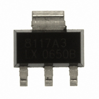
LX8117A-33CST Microsemi Analog Mixed Signal Group, LX8117A-33CST Datasheet - Page 3

LX8117A-33CST
Manufacturer Part Number
LX8117A-33CST
Description
IC REG LDO POS 1A 3.3V SOT223
Manufacturer
Microsemi Analog Mixed Signal Group
Datasheet
1.LX8117-28CST.pdf
(11 pages)
Specifications of LX8117A-33CST
Regulator Topology
Positive Fixed
Voltage - Output
3.3V
Voltage - Input
Up to 15V
Voltage - Dropout (typical)
1.15V @ 1A
Number Of Regulators
1
Current - Limit (min)
1A
Operating Temperature
0°C ~ 125°C
Mounting Type
Surface Mount
Package / Case
SOT-223 (3 leads + Tab), SC-73, TO-261
Lead Free Status / RoHS Status
Lead free / RoHS Compliant
Current - Output
-
Copyright © 1999
Rev. 1.5a
Note 2. Range over which the device is functional.
(Unless otherwise specified: 0°C
LX8117-00 / 8117A-00 / 8117B-00 (Adjustable)
Notes: 3. See thermal regulation specification for changes in output voltage due to heating effects. Load regulation and line regulation are measured at a constant junction
Input Voltage
Input-Output Differential
Operating Ambient Temperature Range
Reference Voltage
Line Regulation (Note 3)
Load Regulation (Note 3)
Dropout Voltage
Current Limit
Minimum Load Current (Note 5)
Thermal Regulation
Ripple Rejection
Adjust Pin Current
Adjust Pin Current Change
Temperature Stability
Long Term Stability
RMS Output Noise (% of V
Operating Voltage
(Note 4)
4. Dropout voltage is specified over the full output current range of the device. Dropout voltage is defined as the minimum input/output differential measured
5. Minimum load current is defined as the minimum output current required to maintain regulation.
temperature by low duty cycle pulse testing.
at the specified output current. Test points and limits are also shown on the Dropout Voltage Curve.
Parameter
LX8117-00
LX8117A/B-00
LX8117-00
LX8117A-00
LX8117B-00
Parameter
OUT
)
R E C O M M E N D E D O P E R AT I N G C O N D I T I O N S
LX8117(A/B)-00 / 8117(A/B)-05
LX8117(A/B)-25 / -28 / -33
LX8117(A/B)-00
T
J
0.8, 1 & 1.2A L
P R O D U C T D A T A B O O K 1 9 9 6 / 1 9 9 7
125°C, I
Symbol
V
I
I
V
OUT (MAX)
V
V
OUT (MIN)
V
V
OUT (RMS)
OUT
REF
REF
OUT
V
OUT
I
ADJ
I
REF
ADJ
(I
(Pwr)
(V
V
P
E L E C T R I C A L C H A R A C T E R I S T I C S
OUT
MAX
(T)
(t) T
IN
(Other Voltage Options on following pages.)
) I
) (V
R O D U C T I O N
= 0.8A for the LX8117-xx, I
I
10mA
I
I
I
I
(V
(V
(V
V
T
f
10mA
10Hz
OUT
OUT
OUT
OUT
OUT
OUT
RIPPLE
IN
A
A
IN
IN
IN
IN
= 25°C, 30ms pulse
= 125°C, 1000 hours
= 10mA, (V
= 10mA, 1.5V
= 100mA
= 500mA
= I
= I
- V
- V
- V
- V
10V
=120Hz, (V
OUT (MAX)
OUT (MAX)
OUT
OUT
OUT
OUT
O W
f
I
I
OUT
) = 3V, 10mA
) = 5V, T
) = 5V, T
) = 5V, T
OUT
10kHz
D
I
I
OUT (MAX)
OUT (MAX)
LX8117-xx/8117A-xx/8117B-xx
IN
R O P O U T
IN
- V
J
J
J
- V
= 25°C
= 25°C
= 25°C
OUT
(V
OUT
, 1.4V
, 1.4V
) = 2V, T
Test Conditions
IN
Symbol
) = 3V, V
- V
D
I
OUT
MAX
OUT
P
A T A
)
(V
O S I T I V E
= 1.0A for the LX8117A-xx, and I
J
(V
I
OUT (MAX)
= 25°C
IN
RIPPLE
IN
7V
- V
- V
OUT
= 1Vp-p
OUT
S
)
)
Recommended Operating Conditions
H E E T
Min.
R
10V
10V
0
E G U L AT O R S
(Note 2)
Typ.
MAX
LX8117 / 17A / 17B-00
1.238
1.225
1000
1200
Min.
800
60
= 1.2A for the LX8117B-xx.)
1.250
1.250
0.003
1200
1500
Typ.
0.05
0.15
0.97
1.00
1.05
1.15
0.08
950
0.5
0.2
0.5
0.3
75
45
Max.
125
15
12
10
1.262
1.270
Max.
1.10
1.15
1.20
1.30
100
0.2
0.4
0.2
5
5
Units
Units
°C
%/W
V
V
V
mA
mA
mA
mA
µA
µA
%
%
dB
%
%
%
V
V
V
V
V
V
3


