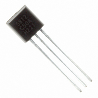
S-812C50AY-B-G Seiko Instruments, S-812C50AY-B-G Datasheet - Page 17

S-812C50AY-B-G
Manufacturer Part Number
S-812C50AY-B-G
Description
IC REG LDO 75MA 5.0V TO-92
Manufacturer
Seiko Instruments
Datasheet
1.S-812C40AMC-C2UT2G.pdf
(53 pages)
Specifications of S-812C50AY-B-G
Regulator Topology
Positive Fixed
Voltage - Output
5V
Voltage - Input
Up to 16V
Voltage - Dropout (typical)
0.12V @ 10mA
Number Of Regulators
1
Current - Output
75mA (Min)
Operating Temperature
-40°C ~ 85°C
Mounting Type
Through Hole
Package / Case
TO-92-3 (Standard Body), TO-226
Number Of Outputs
1
Polarity
Positive
Input Voltage Max
18 V
Output Voltage
5 V
Output Type
Fixed
Dropout Voltage (max)
0.95 V
Output Current
75 mA
Line Regulation
20 mV
Load Regulation
80 mV
Voltage Regulation Accuracy
2 %
Maximum Power Dissipation
800 mW
Maximum Operating Temperature
+ 85 C
Mounting Style
Through Hole
Minimum Operating Temperature
- 40 C
Lead Free Status / RoHS Status
Lead free / RoHS Compliant
Current - Limit (min)
-
Lead Free Status / Rohs Status
Lead free / RoHS Compliant
Other names
728-1026
Rev.5.0
Operation
1. Basic Operation
2. Output Transistor
Figure 16 shows the block diagram of the S-812C Series.
The error amplifier compares the reference voltage (V
divided by feedback resistors R
output voltage which is not influenced by the input voltage and temperature change, to the output
transistor.
In the S-812C Series, a low on-resistance P-channel MOS FET is used as the output transistor.
Be sure that V
to inverse current which flows, because of a parasitic diode between the VIN and VOUT pin.
_00
Current supply
OUT
VSS
VIN
*1. Parasitic diode
does not exceed V
HIGH OPERATING VOLTAGE CMOS VOLTAGE REGULATOR
V
Reference
ref
voltage
circuit
s
and R
Error amplifier
IN
Seiko Instruments Inc.
+ 0.3 V to prevent the voltage regulator from being damaged due
f
. It supplies the gate voltage necessary to maintain the constant
+
−
Figure 16
ref
) with V
fb
R
R
, which is the output voltage resistance-
f
S
*1
VOUT
S-812C Series
17


