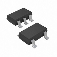
ADP121-AUJZ33R7 Analog Devices Inc, ADP121-AUJZ33R7 Datasheet - Page 12

ADP121-AUJZ33R7
Manufacturer Part Number
ADP121-AUJZ33R7
Description
IC REG LDO 150MA 3.3V TSOT-23-5
Manufacturer
Analog Devices Inc
Datasheet
1.ADP121UJZ-REDYKIT.pdf
(20 pages)
Specifications of ADP121-AUJZ33R7
Design Resources
Low power, Long Range, ISM Wireless Measuring Node (CN0164)
Regulator Topology
Positive Fixed
Voltage - Output
3.3V
Voltage - Input
Up to 5.5V
Voltage - Dropout (typical)
0.12V @ 150mA
Number Of Regulators
1
Current - Output
150mA
Current - Limit (min)
160mA
Operating Temperature
-40°C ~ 125°C
Mounting Type
Surface Mount
Package / Case
TSOT-23-5, TSOT-5, TSOP-5
Primary Input Voltage
3.8V
Output Voltage Adjustable Range
1.2V To 3.3V
Output Voltage Fixed
3.3V
Dropout Voltage Vdo
120mV
No. Of Pins
5
Output Current
150mA
Lead Free Status / RoHS Status
Lead free / RoHS Compliant
Other names
ADP121-AUJZ33R7TR
Available stocks
Company
Part Number
Manufacturer
Quantity
Price
Company:
Part Number:
ADP121-AUJZ33R7
Manufacturer:
LAMBDA
Quantity:
210
Company:
Part Number:
ADP121-AUJZ33R7
Manufacturer:
AD
Quantity:
36 000
ADP121
APPLICATIONS INFORMATION
CAPACITOR SELECTION
Output Capacitor
The ADP121 is designed for operation with small, space-saving
ceramic capacitors, but functions with most commonly used
capacitors as long as care is taken with the effective series resistance
(ESR) value. The ESR of the output capacitor affects stability of the
LDO control loop. A minimum of 0.70 µF capacitance with an
ESR of 1 Ω or less is recommended to ensure stability of the
ADP121. The transient response to changes in the load current is
also affected by output capacitance. Using a larger value of output
capacitance improves the transient response of the ADP121 to
large changes in the load current. Figure 28 and Figure 29 show
the transient responses for output capacitance values of 1 µF and
4.7 µF, respectively.
V
C
OUT
IN
= C
V
C
= 1.8V,
Figure 29. Output Transient Response, C
OUT
IN
Figure 28. Output Transient Response, C
OUT
= C
I
LOAD
= 1.8V,
= 1µF
OUT
= 4.7µF
1mA TO 150mA LOAD STEP,
(400ns/DIV)
1mA TO 150mA LOAD STEP,
I
V
LOAD
2.5A/µs
OUT
(400ns/DIV)
V
OUT
2.5A/µs
OUT
OUT
= 4.7 µF
= 1 µF
CH1 MEAN
115.7mA
Rev. D | Page 12 of 20
Input Bypass Capacitor
Connecting a 1 µF capacitor from VIN to GND reduces the
circuit sensitivity to the PCB layout, especially when long input
traces or high source impedance is encountered. If output
capacitance greater than 1 µF is required, the input capacitor
should be increased to match it.
Input and Output Capacitor Properties
Any good quality ceramic capacitor can be used with the
ADP121, as long as it meets the minimum capacitance and
maximum ESR requirements. Ceramic capacitors are manufac-
tured with a variety of dielectrics, each with a different behavior
over temperature and applied voltage. Capacitors must have an
adequate dielectric to ensure the minimum capacitance over
the necessary temperature range and dc bias conditions. X5R
or X7R dielectrics with a voltage rating of 6.3 V or 10 V are
recomm ended. Y5V and Z5U dielectrics are not
recommended, due to their poor temperature and dc bias
characteristics.
Figure 30 depicts the capacitance vs. voltage bias characteristic
of an 0402 1 µF, 10 V, X5R capacitor. The voltage stability of a
capacitor is strongly influenced by the capacitor size and voltage
rating. In general, a capacitor in a larger package or higher voltage
rating exhibits better stability. The temperature variation of the
X5R dielectric is about ±15% over the −40°C to +85°C tempera-
ture range and is not a function of package or voltage rating.
1.2
1.0
0.8
0.6
0.4
0.2
0
0
Figure 30. Capacitance vs. Voltage Bias Characteristic
2
VOLTAGE (V)
4
6
8
10


