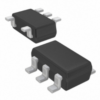
XC6217A302MR Torex Semiconductor Ltd, XC6217A302MR Datasheet - Page 12

XC6217A302MR
Manufacturer Part Number
XC6217A302MR
Description
IC REG LDO 3V .25A SOT-25
Manufacturer
Torex Semiconductor Ltd
Datasheet
1.XC6217A182MR.pdf
(33 pages)
Specifications of XC6217A302MR
Regulator Topology
Positive Fixed
Voltage - Output
3V
Voltage - Input
Up to 6V
Voltage - Dropout (typical)
0.08V @ 100mA
Number Of Regulators
1
Current - Output
200mA (Min)
Current - Limit (min)
200mA
Operating Temperature
-40°C ~ 85°C
Mounting Type
Surface Mount
Package / Case
SOT-23-5, SC-74A, SOT-25
Lead Free Status / RoHS Status
Lead free / RoHS Compliant
Other names
893-1083-2
12/33
<Green Operation>
■OPERATIONAL EXPLANATION
<Output Voltage Control>
XC6217A and B series can be set as a fixed high-speed mode or a green operation (GO) mode via a signal to the green
operation (GO) pin. Under the condition that the GO pin becomes low level, the IC operates in the GO mode and the IC
operates in the fixed high-speed mode when the GO pin is at high level. The GO mode enables the IC to switch
automatically the supply current to the high speed (HS) mode or the power save (PS) mode according to the level of output
current. While having both high-speed operation and low supply current state, the series can acquire high efficiency. At the
HS/PS automatic switching mode (GO mode), the switching point of the HS mode and the PS mode is being fixed inside the
IC. When the output current becomes I
delay time of hundreds μsec(s), and it can reduce supply current in light load. Also when the output current becomes I
8mA (MAX.) or more, the mode changes automatically to the HS mode and the IC becomes high speed operation.
When the XC6217 is used in the GO mode, stable operation range is over 8.0mA is HS mode and below 0.5mA in PS mode.
<Low ESR capacitor>
XC6217
The voltage divided by resistors R1 & R2 is compared with the internal reference voltage by the error amplifier. The
P-channel MOSFET, which is connected to the V
at the V
operate in relation to the level of output current. The GO function monitors the output current and switches a supply current
to two values according to the level of output current. Further, the IC's internal circuitry can be shutdown via the CE pin's
signal.
With the XC6217 series, a stable output voltage is achievable even if used with low ESR capacitors, as a phase
compensation circuit is built-in. Values required for the phase compensation are as the chart below. In order to ensure the
stable phase compensation while avoiding run-out of values, please use the capacitor which does not depend on bias or
temperature too much. For a stable power input, please connect an input capacitor (C
the V
・Excluding USPN-4
・USPN-4
SS
OUT
OUTPUT VOLTAGE (V)
pin.
OUTPUT VOLTAGE (V)
pin is controlled & stabilized by a system of negative feedback. The current limit circuit and short protect circuit
0.8 ~ 1.15
1.2 ~ 1.35
1.4 ~ 4.0
1.6 ~ 4.0
Series
GOR
OUTPUT CAPACITOR VALUE
OUTPUT CAPACITOR VALUE
0.5mA (MIN.) or below, the mode changes automatically to the PS mode after the
More than C
More than C
More than C
More than C
OUT
pin, is then driven by the subsequent output signal. The output voltage
L
L
L
L
=4.7μF
=2.2μF
=1.0μF
=2.2μF
IN
) of 1.0μF between the V
IN
pin and
GO


