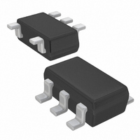
XC6217A252MR Torex Semiconductor Ltd, XC6217A252MR Datasheet - Page 13

XC6217A252MR
Manufacturer Part Number
XC6217A252MR
Description
IC REG LDO 2.5V .25A SOT-25
Manufacturer
Torex Semiconductor Ltd
Datasheet
1.XC6217A182MR.pdf
(33 pages)
Specifications of XC6217A252MR
Regulator Topology
Positive Fixed
Voltage - Output
2.5V
Voltage - Input
Up to 6V
Voltage - Dropout (typical)
0.095V @ 100mA
Number Of Regulators
1
Current - Output
200mA (Min)
Current - Limit (min)
200mA
Operating Temperature
-40°C ~ 85°C
Mounting Type
Surface Mount
Package / Case
SOT-23-5, SC-74A, SOT-25
Lead Free Status / RoHS Status
Lead free / RoHS Compliant
Other names
893-1082-2
Available stocks
Company
Part Number
Manufacturer
Quantity
Price
Company:
Part Number:
XC6217A252MR
Manufacturer:
TOREX
Quantity:
16 950
<C
■NOTES ON USE
<Current Limiter, Short-Circuit Protection>
<CE Pin>
( V : Output voltage after discharge, V
L
τ: C
XC6217B/D series can quickly discharge the electric charge at the output capacitor (C
which enables a whole IC circuit put into OFF state, is inputted via the N-channel transistor located between the V
and the V
typical). The discharge time of the output capacitor (C
capacitor (C
(C
formulas.
Auto-Discharge Function>
1. Please use this IC within the stated absolute maximum ratings. The IC is liable to malfunction should the ratings be
2. Where wiring impedance is high, operations may become unstable due to noise and/or phase lag depending on output current.
3. Please wire the input capacitor (C
The XC6217 series’ foldback circuit operates as an output current limiter and a short protection of the output pin. When
the load current reaches the current limit level, the fixed current limiter circuit operates and output voltage drops. As a
result of this drop in output voltage, the foldback circuit operates, output voltage drops further and output current
decreases. When the output pin is shorted to the V
The IC's internal circuitry can be shutdown via the signal from the CE pin with the XC6217 series. In shutdown mode,
output at the V
auto-discharge resistor is connected in parallel to R1 and R2 while the power supply is applied to the VIN pin.
Therefore, time until the V
CE pin is open. If this IC is used with the correct output voltage for the CE pin, the logic is fixed and the IC will operate
normally. However, supply current may increase as a result of through current in the IC's internal circuitry when medium
voltage is input.
L
) as τ(τ=C x R
exceeded.
Please strengthen V
V = V
L
auto-discharge resistance R
OUT(E)
SS
pin (cf. BLOCK DIAGRAM). The C
L
). By setting time constant of a CL auto-discharge resistance value [R
x e
OUT
–t/ τ
pin will be pulled down to the VSS level via R1 & R2. However, as for the XC6217B/D series, the C
DCHG
, or t=
IN
), the output voltage after discharge via the N channel transistor is calculated by the following
and V
OUT
τ
pin reaches the V
SS
In ( V / V
DCHG
wiring in particular.
OUT(E)
IN
×Output capacitor (C
) and the output capacitor (C
: Output voltage, t: Discharge time,
OUT(E)
L
auto-discharge resistance value is fixed to 780Ω(V
)
SS
level becomes short. The output voltage becomes unstable, when the
SS
level, a current of about 30mA flows.
L
) is set by the C
L
) value C)
L
) as close to the IC as possible.
L
auto-discharge resistance (R) and the output
DCHG
L
), when a low signal to the CE pin,
] and an output capacitor value
IN
=6.0V, V
OUT
=4.0V at
XC6217
OUT
13/33
Series
pin
L


