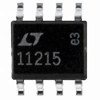
LT1121CS8-5#PBF Linear Technology, LT1121CS8-5#PBF Datasheet - Page 13

LT1121CS8-5#PBF
Manufacturer Part Number
LT1121CS8-5#PBF
Description
IC REG LDO 5V 150MA 8-SOIC
Manufacturer
Linear Technology
Specifications of LT1121CS8-5#PBF
Regulator Topology
Positive Fixed
Voltage - Output
5V
Voltage - Input
Up to 30V
Voltage - Dropout (typical)
0.42V @ 150mA
Number Of Regulators
1
Current - Output
150mA
Operating Temperature
0°C ~ 125°C
Mounting Type
Surface Mount
Package / Case
8-SOIC (3.9mm Width)
Primary Input Voltage
30V
Output Voltage Fixed
5V
Dropout Voltage Vdo
420mV
No. Of Pins
8
Output Current
150mA
Operating Temperature Range
0°C To +125°C
Msl
MSL 1 - Unlimited
Rohs Compliant
Yes
Lead Free Status / RoHS Status
Lead free / RoHS Compliant
Current - Limit (min)
-
Available stocks
Company
Part Number
Manufacturer
Quantity
Price
APPLICATIO S I FOR ATIO
A 7.5k resistor is in series with the output so that it can be
easily overdriven by an external reference or other
circuitry (see Figure 12b). The reference amplifier gains
the voltage at the V
internal reference voltage. This provides buffering
between the V
The reference amplifier compensation pin (REFCOMP, Pin
4) must be bypassed with a capacitor to ground. The
reference amplifier is stable with capacitors of 22 F or
greater. Using a 0.1 F ceramic in parallel is recommended.
The V
shown in Figure 13. This is useful in applications where the
peak input signal amplitude may vary. The input span of
the ADC can then be adjusted to match the peak input
signal, maximizing the signal-to-noise ratio. The filtering
of the internal LTC1608 reference amplifier will limit
the bandwidth and settling time of this circuit. A settling
time of 20ms should be allowed for after a reference
adjustment.
Figure 12b. Using the LT1019-2.5 as an External Reference
4.375V
REF
2.500V
pin can be driven with a DAC or other means
LT1019A-2.5
22 F
Figure 12a. LTC1608 Reference Circuit
3
4
5
V
5V
IN
REF
V
REFCOMP
AGND
V
REF
OUT
pin and the high speed capacitive DAC.
+
U
REF
22 F
ANALOG
pin by 1.75 to create the required
INPUT
16k
R3
U
REFERENCE
12k
R2
AMP
0.1 F
1
2
3
4
5
A
A
V
W
REFCOMP
AGND
IN
IN
REF
+
–
LTC1608
7.5k
R1
REFERENCE
BANDGAP
1608 F12b
LTC1608
U
1608 F12a
Differential Inputs
The LTC1608 has a unique differential sample-and-hold
circuit that allows rail-to-rail inputs. The ADC will always
convert the difference of A
common mode voltage (see Figure 15a). The common
mode rejection holds up to extremely high frequencies
(see Figure 14a). The only requirement is that both inputs
can not exceed the AV
Integral nonlinearity errors (INL) and differential nonlin-
earity errors (DNL) are independent of the common mode
voltage, however, the bipolar zero error (BZE) will vary.
The change in BZE is typically less than 0.1% of the
common mode voltage. Dynamic performance is also
affected by the common mode voltage. THD will degrade
as the inputs approach either power supply rail, from 96dB
with a common mode of 0V to 86dB with a common mode
of 2.5V or – 2.5V.
LTC1450
Figure 14a. CMRR vs Input Frequency
80
70
60
50
40
30
20
10
0
Figure 13. Driving V
1k
INPUT FREQUENCY (Hz)
DD
ANALOG INPUT
10k
DIFFERENTIAL
2V TO 2.7V
2V TO 2.7V
or V
IN
+
22 F
SS
– A
REF
100k
power supply voltages.
IN
with a DAC
1
2
3
4
5
–
A
A
V
REFCOMP
AGND
independent of the
IN
IN
REF
+
–
1608 G14a
LTC1608
LTC1608
1M
1608 F13
13


