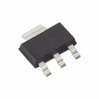
ZSR330GTA Diodes Zetex, ZSR330GTA Datasheet

ZSR330GTA
Specifications of ZSR330GTA
Related parts for ZSR330GTA
ZSR330GTA Summary of contents
Page 1
... A. Output voltage change, with input voltage and load current, is much lower than competitive devices. The ZSR devices are completely stable with no external components. SOT223 ordering information Order reference Voltage ZSR300GTA 3.0V ZSR330GTA 3.3V ZSR500GTA 5.0V ZSR800GTA 8.0V ZSR1000GTA 10.0V ZSR1200GTA 12.0V Issue 9 - October 2007 © ...
Page 2
Absolute maximum rating Input voltage Output current ( Operating temperature Storage temperature Recommended operating conditions Parameter Products ZSR300 ZSR330 V Input Voltage ZSR500 in ZSR800 ZSR1000 ZSR1200 Notes: • The maximum operating input voltage and output current of ...
Page 3
Electrical characteristics ZSR300 test conditions (Unless otherwise stated):T Symbol Parameter V Output Voltage O V Line regulation O V Load regulation O I Quiescent current g I Quiescent current change Output noise voltage ...
Page 4
ZSR500 test conditions (Unless otherwise stated):T Symbol Parameter V Output Voltage O V Line regulation O V Load regulation O I Quiescent current g I Quiescent current change Output noise voltage Ripple rejection ...
Page 5
ZSR1000 test conditions (Unless otherwise stated):T Symbol Parameter V Output Voltage O V Line regulation O V Load regulation O I Quiescent current g I Quiescent current change Output noise voltage Ripple rejection ...
Page 6
Schematic diagram Applications Issue 9 - October 2007 © Zetex Semiconductors plc 2007 ZSR SERIES 6 www.zetex.com ...
Page 7
Typical characteristics Issue 9 - October 2007 © Zetex Semiconductors plc 2007 ZSR SERIES 7 www.zetex.com ...
Page 8
Typical characteristics 3.01 3.00 2.99 2.98 2.86 2.85 2.84 ZSR285 2.82 -50 - Temperature (°C) Output Voltage Temperature Coefficient 9.08 ZSR900 9.04 9.00 8.96 8.92 -50 - Temperature (°C) Output Voltage Temperature Coefficient 500 400 300 ...
Page 9
Typical characteristics Issue 9 - October 2007 © Zetex Semiconductors plc 2007 ZSR SERIES 9 www.zetex.com ...
Page 10
Typical characteristics Issue 9 - October 2007 © Zetex Semiconductors plc 2007 ZSR SERIES 10 www.zetex.com ...
Page 11
Typical characteristics Issue 9 - October 2007 © Zetex Semiconductors plc 2007 ZSR SERIES 11 www.zetex.com ...
Page 12
Typical characteristics Issue 9 - October 2007 © Zetex Semiconductors plc 2007 ZSR SERIES 12 www.zetex.com ...
Page 13
Typical characteristics Issue 9 - October 2007 © Zetex Semiconductors plc 2007 ZSR SERIES 13 www.zetex.com ...
Page 14
Obsolete Variants TO92 Package suffix - C IN GND OUT Underside view SOT223 Order information Orderable Voltage ZSR285GTA 2.85V ZSR400GTA 4.0V ZSR485GTA 4.85V ZSR520GTA 5.2V ZSR600GTA 6.0V ZSR900GTA 9.0V TO92 Order information Part Number Voltage ZSR285 2.85V ZSR300 3.0V ZSR330 ...
Page 15
ZSR285 test conditions Symbol Parameter V Output Voltage O V Line regulation O V Load regulation O I Quiescent current g I Quiescent current change Output noise voltage Ripple rejection ...
Page 16
ZSR485 test conditions (Unless otherwise stated):T V Output Voltage O V Line regulation O V Load regulation O I Quiescent current g I Quiescent current change Output noise voltage Ripple rejection in O ...
Page 17
ZSR600 test conditions (Unless otherwise stated):T Symbol Parameter V Output Voltage O V Line regulation O V Load regulation O I Quiescent current g I Quiescent current change Output noise voltage Ripple rejection ...
Page 18
Definitions Product change Zetex Semiconductors reserves the right to alter, without notice, specifications, design, price or conditions of supply of any product or service. Customers are solely responsible for obtaining the latest relevant information before placing orders. Applications disclaimer The ...


