AP1117K50L-13 Diodes Inc, AP1117K50L-13 Datasheet - Page 4
AP1117K50L-13
Manufacturer Part Number
AP1117K50L-13
Description
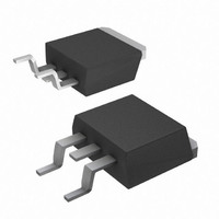
IC REG LDO 1.0A 5.0V TO263-3L
Manufacturer
Diodes Inc
Datasheet
1.AP1117D33G-13.pdf
(11 pages)
Specifications of AP1117K50L-13
Regulator Topology
Positive Fixed
Voltage - Output
5V
Voltage - Input
Up to 18V
Voltage - Dropout (typical)
1.3V @ 1A
Number Of Regulators
1
Current - Output
1A
Current - Limit (min)
1.1A
Operating Temperature
0°C ~ 125°C
Mounting Type
Surface Mount
Package / Case
TO-263-2, D⊃2Pak (2 leads + Tab), TO-263AB
Number Of Outputs
1
Polarity
Positive
Input Voltage Max
18 V
Output Voltage
5 V
Output Type
Fixed
Dropout Voltage (max)
1.4 V at 1 A
Output Current
1 A
Line Regulation
0.2 %
Load Regulation
50 mV
Maximum Power Dissipation
15 W
Maximum Operating Temperature
+ 125 C
Mounting Style
SMD/SMT
Minimum Operating Temperature
- 40 C
Lead Free Status / RoHS Status
Lead free / RoHS Compliant
Other names
AP1117K50LDITR
Available stocks
Company
Part Number
Manufacturer
Quantity
Price
Company:

Part Number:
AP1117K50L-13
Manufacturer:
Diodes Inc
Quantity:
1 938


Electrical Characteristics
Notes:
AP1117
Document number: DS31009 Rev. 20 - 2
Load Regulation
(cont.)
Dropout Voltage
(V
Dropout Voltage
(V
Current Limit
Minimum Load Current
(Note 5)
Thermal Regulation
Ripple Rejection
Temperature Stability
θ
Junction-to-Ambient θ
θ
Junction-to-Case
JA
JC
IN
IN
Thermal Resistance
Thermal Resistance
-V
-V
OUT
OUT
Parameter
3.See thermal regulation specifications for changes in output voltage due to heating effects. Line and load regulation are measured at a constant
4. Line and load regulation are guaranteed up to the maximum power dissipation of 15W. Power dissipation is determined by the difference
5. Quiescent current is defined as the minimum output current required in maintaining regulation. At 12V input/output differential the
6. Test conditions for SOT89-3L, TO220-3L, TO252-3L and TO263-3L: Devices mounted on FR-4 substrate, single sided PC board, 2oz copper, with
7. Test conditions for SOT223-3L: Devices mounted on FR-4 substrate, single sided PC board, 2oz copper, with 5mmx5mm thermal pad layout, no
)
)
junction temperature by low duty cycle pulse testing. Load regulation is measured at the output lead = 1/18” from the package.
between input and output differential and the output current. Guaranteed maximum power dissipation will not be available over the full input/output
range.
device is guaranteed to regulate if the output current is greater than 10mA.
minimum recommended pad layout, no air flow. The case point of θ
air flow. The case point of θ
JA
AP1117-3.3
AP1117-5.0
AP1117-ADJ/1.5/1.8
/2.5/3.3/5.0
AP1117-ADJ/1.5/1.8
/2.5/3.3/5.0
AP1117-ADJ/1.5/1.8
/2.5/3.3/5.0
AP1117-XXX
T
F = 180Hz, C
AP1117-XXX
I
SOT89-3L: Control Circuitry/Power Transistor (Note 6)
SOT223-3L: Control Circuitry/Power Transistor (Note 7)
TO252-3L: Control Circuitry/Power Transistor (Note 6)
TO220-3L: Control Circuitry/Power Transistor (Note 6)
TO263-3L: Control Circuitry/Power Transistor (Note 6)
SOT89-3L: Control Circuitry/Power Transistor (Note 6)
SOT223-3L: Control Circuitry/Power Transistor (Note 7)
TO252-3L: Control Circuitry/Power Transistor (Note 6)
TO220-3L: Control Circuitry/Power Transistor (Note 6)
TO263-3L: Control Circuitry/Power Transistor (Note 6)
O
A
= 10mA
= 25
JC
o
C, 30ms pulse
is located on the thermal tab.
(Under Operating Conditions)
OUT
= 25uF Tantalum, I
V
Conditions
IN
V
T
V
T
I
0
I
0
(V
0
OUT
OUT
= V
o
o
o
A
A
IN
IN
C ≤ T
C ≤ T
C ≤ T
IN
= 25
= 25
= 5V, 0 ≤ I
= 8V, 0 ≤ I
-V
OUT
= 800mA, ΔV
= 1A, ΔV
OUT
o
o
J
J
J
www.diodes.com
+3V
C (Note 3, 4)
C (Note 3, 4)
≤ 125
≤ 125
≤ 125
) = 5V
4 of 11
OUT
OUT
OUT
OUT
o
o
o
1A LOW DROPOUT POSITIVE ADJUSTABLE
C
C
C
JC
is located on the thermal tab.
= 1%V
OUT
≤ 1A,
≤ 1A,
= 1A
= 1%V
OUT
(cont.)
OUT
OR FIXED-MODE REGULATOR
Min
1. 1
0.008
Typ.
164
107
1.2
1.3
0.5
3.5
3.5
26
40
60
73
78
60
42
15
12
5
AP1117
Max
0.04
© Diodes Incorporated
1.3
1.4
33
50
10
70
March 2011
°C/W
°C/W
%/W
Unit
mV
mV
mA
dB
%
V
V
A
Related parts for AP1117K50L-13
Image
Part Number
Description
Manufacturer
Datasheet
Request
R

Part Number:
Description:
Diodes (General Purpose, Power, Switching) 240V 350mW
Manufacturer:
Diodes Inc
Datasheet:

Part Number:
Description:
Diodes (General Purpose, Power, Switching) -
Manufacturer:
Diodes Inc
Part Number:
Description:
Diodes (General Purpose, Power, Switching) -
Manufacturer:
Diodes Inc

Part Number:
Description:
Diodes (General Purpose, Power, Switching) NPN Small SIG 50V 45V VCEO 6.0V VEBO
Manufacturer:
Diodes Inc
Datasheet:
Part Number:
Description:
Diodes (General Purpose, Power, Switching) NPN Small SIG 30V 30V VCEO 5.0V VEBO
Manufacturer:
Diodes Inc
Datasheet:
Part Number:
Description:
Diodes (General Purpose, Power, Switching) NPN Small SIG -80V -65V VCEO -5.0 VEBO
Manufacturer:
Diodes Inc
Datasheet:
Part Number:
Description:
Diodes (General Purpose, Power, Switching) NPN Small SIG -50V -45V VCEO 6.0V VEBO
Manufacturer:
Diodes Inc
Part Number:
Description:
Diodes (General Purpose, Power, Switching) Dual Switching DIODE 100V Vrm 75Vrrm 53Vr
Manufacturer:
Diodes Inc
Datasheet:

Part Number:
Description:
Diodes (General Purpose, Power, Switching) Vr/80V Io/125mA T/R
Manufacturer:
Diodes Inc
Datasheet:

Part Number:
Description:
Diodes (General Purpose, Power, Switching) HV DUAL SW DIODE 300V
Manufacturer:
Diodes Inc
Datasheet:

Part Number:
Description:
Diodes (General Purpose, Power, Switching) 80V 150mW
Manufacturer:
Diodes Inc
Datasheet:
Part Number:
Description:
Diodes (General Purpose, Power, Switching) 75V 150mW
Manufacturer:
Diodes Inc
Datasheet:

Part Number:
Description:
Diodes (General Purpose, Power, Switching) 200MW 80V
Manufacturer:
Diodes Inc
Part Number:
Description:
Diodes (General Purpose, Power, Switching) 100V Io/150mA T/R INVALID P/N
Manufacturer:
Diodes Inc

Part Number:
Description:
Diodes (General Purpose, Power, Switching) 350MW 75V
Manufacturer:
Diodes Inc