AP7165-FNG-7 Diodes Inc, AP7165-FNG-7 Datasheet - Page 9
AP7165-FNG-7
Manufacturer Part Number
AP7165-FNG-7
Description
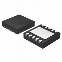
IC REG LDO 600MA POK 10-DFN
Manufacturer
Diodes Inc
Datasheet
1.AP7165-FNG-7.pdf
(14 pages)
Specifications of AP7165-FNG-7
Regulator Topology
Positive Adjustable
Voltage - Output
0.8 ~ 5 V
Voltage - Input
2.2 ~ 5.5 V
Voltage - Dropout (typical)
0.3V @ 500mA
Number Of Regulators
1
Current - Output
600mA (Max)
Current - Limit (min)
600mA
Operating Temperature
-40°C ~ 85°C
Mounting Type
Surface Mount
Package / Case
10-DFN
Number Of Outputs
1
Polarity
Positive
Input Voltage Max
5.5 V
Output Voltage
0.8 V to 5 V
Output Type
Adjustable
Dropout Voltage (max)
0.4 V at 500 mA
Output Current
600 mA
Line Regulation
0.015 % / V
Load Regulation
1 %
Voltage Regulation Accuracy
2.5 %
Maximum Power Dissipation
3.1 W
Maximum Operating Temperature
+ 85 C
Mounting Style
SMD/SMT
Minimum Operating Temperature
- 40 C
Reference Voltage
0.8 V
Lead Free Status / RoHS Status
Lead free / RoHS Compliant
Other names
AP7165-FNGDITR


Application Notes
Input Capacitor
A 1 μ F ceramic capacitor is recommended to connect
between IN and GND pins to decouple input power supply
glitch and noise. The amount of the capacitance may be
increased without limit. A lower ESR (Equivalent Series
Resistance) capacitor allows the use of less capacitance,
while higher ESR type requires more capacitance. This
input capacitor should be located as close as possible to
the device to assure input stability and less noise. For
PCB layout, a wide copper trace is required for both IN
and GND.
Output Capacitor
The output capacitor is required to stabilize and help the
transient response of the LDO. The AP7165 is designed to
have excellent transient response for most applications
with a small amount of output capacitance. The AP7165 is
stable for all available types and values of output
capacitors ≥ 4.7 μ F. The device is also stable with multiple
capacitors in parallel, which can be of any type of value.
Additional capacitance helps to reduce undershoot and
overshoot during transient. This capacitor should be
placed as close as possible to OUT and GND pins for
optimum performance.
Adjustable Operation
The AP7165 provides output voltage from 0.8V to 5.0V
through external resistor divider as shown below.
The output voltage is calculated by:
Where V
AP7165
Document number: DS31270 Rev. 6 - 2
V
IN
C
REF
IN
=0.8V (the internal reference voltage).
100kOhm
Enable
V
OUT
POK
EN
IN
=
V
AP7165
REF
⎛
⎜ ⎜
⎝
1
OUT
GND
FB
+
R
R
2
1
R
R
⎞
⎟ ⎟
⎠
1
2
V
OUT
C
OUT
www.diodes.com
600mA LOW DROPOUT REGULATOR WITH POK
9 of 14
Rearranging the equation will give the following equation
to find the approximate resistor divider values:
To maintain the stability of the internal reference voltage,
R
No Load Stability
Other than external resistor divider, no minimum load is
required to keep the device stable. The device will remain
stable and regulated in no load condition.
ENABLE/SHUTDOWN Operation
The AP7165 is turned on by setting the EN pin high, and is
turned off by pulling it low. If this feature is not used, the
EN pin should be tied to IN pin to keep the regulator output
on at all time. To ensure proper operation, the signal
source used to drive the EN pin must be able to swing
above and below the specified turn-on/off voltage
thresholds listed in the Electrical Characteristics section
under V
POWER-OK
The Power-Ok (POK) pin is an active high open-drain
output. It can be connected to any 5.5V or lower rail
through an external pull-up resistor. The recommended
sink current of POK pin is up to 4mA, so the pull-up
resistor for POK should be in the range of 10kΩ to 1MΩ. If
output voltage monitoring is not needed, the POK pin can
be left floating.
Current Limit Protection
When output current at OUT pin is higher than current limit
threshold, the current limit protection will be triggered and
clamp the output current to approximately 950mA (600A
min) to prevent over-current and to protect the regulator
from damage due to overheating.
Short Circuit Protection
When OUT pin is short-circuited to GND or OUT pin
voltage is less than 200mV, short circuit protection will be
triggered and clamp the output current to approximately
380mA. This feature protects the regulator from over-
current and damage due to overheating.
2
needs to be kept smaller than 250k Ω .
IL
and V
IH
R
.
1
=
R
2
⎛
⎜ ⎜
⎝
V
V
OUT
REF
−
1
AP7165
⎞
⎟ ⎟
⎠
© Diodes Incorporated
September 2010
Related parts for AP7165-FNG-7
Image
Part Number
Description
Manufacturer
Datasheet
Request
R

Part Number:
Description:
IC REG LDO 600MA ADJ VOLT 8-SOIC
Manufacturer:
Diodes Inc
Datasheet:

Part Number:
Description:
Diodes (General Purpose, Power, Switching) 240V 350mW
Manufacturer:
Diodes Inc
Datasheet:

Part Number:
Description:
Diodes (General Purpose, Power, Switching) -
Manufacturer:
Diodes Inc
Part Number:
Description:
Diodes (General Purpose, Power, Switching) -
Manufacturer:
Diodes Inc

Part Number:
Description:
Diodes (General Purpose, Power, Switching) NPN Small SIG 50V 45V VCEO 6.0V VEBO
Manufacturer:
Diodes Inc
Datasheet:
Part Number:
Description:
Diodes (General Purpose, Power, Switching) NPN Small SIG 30V 30V VCEO 5.0V VEBO
Manufacturer:
Diodes Inc
Datasheet:
Part Number:
Description:
Diodes (General Purpose, Power, Switching) NPN Small SIG -80V -65V VCEO -5.0 VEBO
Manufacturer:
Diodes Inc
Datasheet:
Part Number:
Description:
Diodes (General Purpose, Power, Switching) NPN Small SIG -50V -45V VCEO 6.0V VEBO
Manufacturer:
Diodes Inc
Part Number:
Description:
Diodes (General Purpose, Power, Switching) Dual Switching DIODE 100V Vrm 75Vrrm 53Vr
Manufacturer:
Diodes Inc
Datasheet:

Part Number:
Description:
Diodes (General Purpose, Power, Switching) Vr/80V Io/125mA T/R
Manufacturer:
Diodes Inc
Datasheet:

Part Number:
Description:
Diodes (General Purpose, Power, Switching) HV DUAL SW DIODE 300V
Manufacturer:
Diodes Inc
Datasheet:

Part Number:
Description:
Diodes (General Purpose, Power, Switching) 80V 150mW
Manufacturer:
Diodes Inc
Datasheet:
Part Number:
Description:
Diodes (General Purpose, Power, Switching) 75V 150mW
Manufacturer:
Diodes Inc
Datasheet:

Part Number:
Description:
Diodes (General Purpose, Power, Switching) 200MW 80V
Manufacturer:
Diodes Inc
Part Number:
Description:
Diodes (General Purpose, Power, Switching) 100V Io/150mA T/R INVALID P/N
Manufacturer:
Diodes Inc