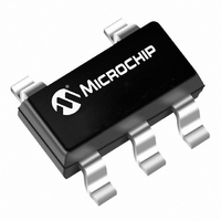
TC1014-3.3VCT713 Microchip Technology, TC1014-3.3VCT713 Datasheet - Page 11

TC1014-3.3VCT713
Manufacturer Part Number
TC1014-3.3VCT713
Description
IC CMOS LDO 3.3V 50MA SOT23-5
Manufacturer
Microchip Technology
Specifications of TC1014-3.3VCT713
Package / Case
SOT-23-5, SC-74A, SOT-25
Regulator Topology
Positive Fixed
Voltage - Output
3.3V
Voltage - Input
Up to 6V
Voltage - Dropout (typical)
0.085V @ 50mA
Number Of Regulators
1
Current - Output
50mA (Min)
Operating Temperature
-40°C ~ 125°C
Mounting Type
Surface Mount
Number Of Outputs
1
Polarity
Positive
Input Voltage Max
6 V
Output Voltage
3.3 V
Output Type
Fixed
Dropout Voltage (max)
250 / 400 mV
Output Current
50 mA
Line Regulation
0.05 %
Load Regulation
0.5 %
Voltage Regulation Accuracy
2.5 %
Maximum Operating Temperature
+ 125 C
Mounting Style
SMD/SMT
Minimum Operating Temperature
- 40 C
Lead Free Status / RoHS Status
Lead free / RoHS Compliant
Current - Limit (min)
-
Lead Free Status / Rohs Status
Lead free / RoHS Compliant
Other names
TC1014-3.3VCT713
TC1014-3.3VCT713TR
TC10143.3VCT713
TC1014-3.3VCT713TR
TC10143.3VCT713
Available stocks
Company
Part Number
Manufacturer
Quantity
Price
Company:
Part Number:
TC1014-3.3VCT713
Manufacturer:
TI
Quantity:
1 492
Part Number:
TC1014-3.3VCT713
Manufacturer:
MICROCHIP/微芯
Quantity:
20 000
3.0
The descriptions of the pins are listed in
TABLE 3-1:
3.1
Connect the V
voltage. Like all low dropout linear regulators, low
source impedance is necessary for the stable
operation of the LDO. The amount of capacitance
required to ensure low source impedance will
depend on the proximity of the input source
capacitors or battery type. For most applications,
1.0 µF of capacitance will ensure stable operation
of the LDO circuit. The type of capacitor used can
be ceramic, tantalum or aluminum electrolytic.
The low Effective Series Resistance (ESR) char-
acteristics of the ceramic will yield better noise
and Power Supply Ripple Rejection (PSRR)
performance at high frequency.
3.2
Connect the ground pin to the input voltage
return. For the optimal noise and PSRR
performance, the GND pin of the LDO should be
tied to a quiet circuit ground. For applications
have switching or noisy inputs tie the GND pin to
the return of the output capacitor. Ground planes
help lower inductance and voltage spikes caused
by
recommended for applications that are subjected
to fast load transients.
© 2007 Microchip Technology Inc.
(5-Pin SOT-23)
fast
Pin No.
PIN DESCRIPTIONS
1
2
3
4
5
Input Voltage (V
Ground Terminal (GND)
transient
IN
PIN FUNCTION TABLE
pin to the unregulated source
Symbol
Bypass
SHDN
V
GND
V
OUT
load
IN
IN
)
currents
Unregulated supply input.
Ground terminal.
Shutdown control input. The regulator is fully enabled when a logic high is applied to
this input. The regulator enters shutdown when a logic low is applied to this input.
During shutdown, output voltage falls to zero and supply current is reduced to
0.5 µA (maximum).
Reference bypass input. Connecting a 470 pF to this input further reduces output
noise.
Regulated voltage output.
Table
and
3-1.
are
TC1014/TC1015/TC1185
3.3
The Shutdown input is used to turn the LDO on
and off. When the SHDN pin is at a logic high
level, the LDO output is enabled. When the
SHDN pin is pulled to a logic low, the LDO output
is disabled. When disabled, the quiescent current
used by the LDO is less than 0.5 µA max.
3.4
Connecting a low-value ceramic capacitor to the
Bypass pin will further reduce output voltage
noise and improve the PSRR performance of the
LDO. While smaller and larger values can be
used, these affect the speed at which the LDO
output voltage rises when the input power is
applied. The larger the bypass capacitor, the
slower the output voltage will rise.
3.5
Connect the output load to V
connect one side of the LDO output capacitor as
close as possible to the V
Description
Shutdown (SHDN)
Bypass
Output Voltage (V
OUT
OUT
OUT
pin.
of the LDO. Also
DS21335E-page 11
)


