AP7217D-12YG-13 Diodes Inc, AP7217D-12YG-13 Datasheet - Page 7
AP7217D-12YG-13
Manufacturer Part Number
AP7217D-12YG-13
Description
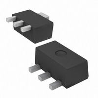
IC REG LDO 1.2V 600MA SOT89-3
Manufacturer
Diodes Inc
Datasheet
1.AP7217D-12YG-13.pdf
(9 pages)
Specifications of AP7217D-12YG-13
Regulator Topology
Positive Fixed
Voltage - Output
1.2V
Voltage - Input
2.5 ~ 5.5 V
Voltage - Dropout (typical)
0.85V @ 600mA
Number Of Regulators
1
Current - Output
600mA (Max)
Operating Temperature
-40°C ~ 85°C
Mounting Type
Surface Mount
Package / Case
SC-62, SOT-89, TO-243 (3 Leads + Tab)
Number Of Outputs
1
Polarity
Positive
Input Voltage Max
5.5 V
Output Voltage
1.2 V
Output Type
Fixed
Dropout Voltage (max)
1.3 V at 600 mA
Output Current
600 mA
Line Regulation
0.2 % / V
Load Regulation
55 mV
Maximum Power Dissipation
0.578 W
Maximum Operating Temperature
+ 85 C
Mounting Style
SMD/SMT
Minimum Operating Temperature
- 40 C
Lead Free Status / RoHS Status
Lead free / RoHS Compliant
Current - Limit (min)
-
Lead Free Status / Rohs Status
Lead free / RoHS Compliant
Other names
AP7217D-12YGDITR
Available stocks
Company
Part Number
Manufacturer
Quantity
Price

Part Number:
AP7217D-12YG-13
Manufacturer:
DIODES/美台
Quantity:
20 000


Application Information
Input Capacitor
A 1μF ceramic capacitor is recommended to connect between IN
and GND pins to decouple input power supply glitch and noise.
The amount of the capacitance may be increased without limit.
A lower ESR (Equivalent Series Resistance) capacitor allows the
use of less capacitance, while higher ESR type requires more
capacitance. This input capacitor must be located as close as
possible to the device to assure input stability and less noise. For
PCB layout, a wide copper trace is required for both IN and GND.
Output Capacitor
The output capacitor is required to stabilize and help the transient
response of the LDO. The AP7217D is designed to have
excellent transient response for most applications with a small
amount of output capacitance. The AP7217D is stable with any
small ceramic output capacitors of 1.0μF or higher value, and the
temperature coefficients of X7R or X5R type.
capacitance helps to reduce undershoot and overshoot during
transient. For PCB layout, the output capacitor must be placed as
close as possible to OUT and GND pins, and keep the leads as
short as possible.
Thermal Considerations
Thermal Shutdown Protection limits power dissipation in
AP7217D. When the operation junction temperature exceeds
150°C, the Over Temperature Protection circuit starts the thermal
shutdown function and turns the pass element off. The pass
element turn on again after the junction temperature cools by
30°C. For continuous operation, do not exceed recommend
maximum operation junction temperature 125°C. The power
dissipation definition in device is:
P
AP7217D Rev. 2
D
= (V
IN
− V
OUT
) x I
OUT
+ V
IN
x I
Q
www.diodes.com
Additional
7 of 9
The maximum power dissipation depends on the thermal
resistance of IC package, PCB layout, the rate of surroundings
airflow and temperature difference between junctions to ambient.
The maximum power dissipation can be calculated by following
formula:
P
Where T
125°C, T
to ambient thermal resistance.
Current Limit Protection
When output current at OUT pin is higher than current limit
threshold, the current limit protection will be triggered and clamp
the output current to approximately 850mA to prevent
over-current and to protect the regulator from damage due to
overheating.
Short circuit protection
When V
200mV, short circuit protection will be triggered and clamp the
output current to approximately 200mA.
D(MAX)
V
IN
OUT
A
= ( T
J(MAX)
is the ambient temperature and the θ
pin is shorted to GND or V
C
I
J(MAX)
is the maximum operation junction temperature
IN
IN
- TA ) / θ
1.2V 600mA CMOS LDO
IN
AP7217D
GND
JA
Iq
OUT
AP7217D
OUT
©
FEBRUARY 2009
voltage is less than
Diodes Incorporated
JA
is the junction
I
OUT
ESR
C
OUT
V
OUT
Related parts for AP7217D-12YG-13
Image
Part Number
Description
Manufacturer
Datasheet
Request
R

Part Number:
Description:
IC REG LDO 500MA 3.3V 8-SOIC
Manufacturer:
Diodes Inc
Datasheet:

Part Number:
Description:
500ma Cmos Ldo
Manufacturer:
Diodes, Inc.
Datasheet:

Part Number:
Description:
500mA CMOS LDO
Manufacturer:
DIODES [Diodes Incorporated]
Datasheet:

Part Number:
Description:
Diodes (General Purpose, Power, Switching) 240V 350mW
Manufacturer:
Diodes Inc
Datasheet:

Part Number:
Description:
Diodes (General Purpose, Power, Switching) -
Manufacturer:
Diodes Inc
Part Number:
Description:
Diodes (General Purpose, Power, Switching) -
Manufacturer:
Diodes Inc

Part Number:
Description:
Diodes (General Purpose, Power, Switching) NPN Small SIG 50V 45V VCEO 6.0V VEBO
Manufacturer:
Diodes Inc
Datasheet:
Part Number:
Description:
Diodes (General Purpose, Power, Switching) NPN Small SIG 30V 30V VCEO 5.0V VEBO
Manufacturer:
Diodes Inc
Datasheet:
Part Number:
Description:
Diodes (General Purpose, Power, Switching) NPN Small SIG -80V -65V VCEO -5.0 VEBO
Manufacturer:
Diodes Inc
Datasheet:
Part Number:
Description:
Diodes (General Purpose, Power, Switching) NPN Small SIG -50V -45V VCEO 6.0V VEBO
Manufacturer:
Diodes Inc
Part Number:
Description:
Diodes (General Purpose, Power, Switching) Dual Switching DIODE 100V Vrm 75Vrrm 53Vr
Manufacturer:
Diodes Inc
Datasheet:

Part Number:
Description:
Diodes (General Purpose, Power, Switching) Vr/80V Io/125mA T/R
Manufacturer:
Diodes Inc
Datasheet:

Part Number:
Description:
Diodes (General Purpose, Power, Switching) HV DUAL SW DIODE 300V
Manufacturer:
Diodes Inc
Datasheet:

Part Number:
Description:
Diodes (General Purpose, Power, Switching) 80V 150mW
Manufacturer:
Diodes Inc
Datasheet:
Part Number:
Description:
Diodes (General Purpose, Power, Switching) 75V 150mW
Manufacturer:
Diodes Inc
Datasheet: