X40626V14-2.7AT1 Intersil, X40626V14-2.7AT1 Datasheet - Page 13

X40626V14-2.7AT1
Manufacturer Part Number
X40626V14-2.7AT1
Description
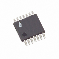
IC SUPERVISOR CPU DUAL 14-TSSOP
Manufacturer
Intersil
Type
Multi-Voltage Supervisorr
Datasheet
1.X40626S14.pdf
(22 pages)
Specifications of X40626V14-2.7AT1
Number Of Voltages Monitored
2
Output
Open Drain or Open Collector
Reset
Active Low
Reset Timeout
100 ms Minimum
Voltage - Threshold
2.23V, 2.93V
Operating Temperature
0°C ~ 70°C
Mounting Type
Surface Mount
Package / Case
14-TSSOP
Lead Free Status / RoHS Status
Contains lead / RoHS non-compliant
Figure 14. Sequential Read Sequence
X40626 Addressing
Slave Address Byte
Following a start condition, the master must output a
Slave Address Byte. This byte consists of several
parts:
– a device type identifier that is ‘1010’ to access the
– one bit of ‘0’.
– next two bits are the device address. (S1 and S0)
– one bit of the slave command byte is a R/W bit. The
array
R/W bit of the Slave Address Byte defines the oper-
ation to be performed. When the R/W bit is a one,
then a read operation is selected. A zero selects a
write operation. Refer to Figure 15.
Signals from
Signals from
the Slave
the Master
SDA Bus
13
S
Address
1
Slave
S
0
1
A
C
K
Data
(1)
A
C
K
X40626
Data
(2)
– After loading the entire Slave Address Byte from the
Word Address
The word address is either supplied by the master or
obtained from an internal counter. The internal counter
is 00H on a power-up condition.
The master must supply the two word address byte as
shown in Figure 15.
SDA bus, the device compares the input slave byte
data to the proper slave byte. Upon a correct compare,
the device outputs an acknowledge on the SDA line.
C
A
K
(n is any integer greater than 1)
Data
(n-1)
A
C
K
Data
(n)
March 28, 2005
S
o
p
t
FN8119.0


