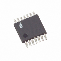
X40626V14-2.7 Intersil, X40626V14-2.7 Datasheet - Page 6

X40626V14-2.7
Manufacturer Part Number
X40626V14-2.7
Description
IC SUPERVISOR CPU DUAL 14-TSSOP
Manufacturer
Intersil
Type
Multi-Voltage Supervisorr
Datasheet
1.X40626S14.pdf
(22 pages)
Specifications of X40626V14-2.7
Number Of Voltages Monitored
2
Output
Open Drain or Open Collector
Reset
Active Low
Reset Timeout
100 ms Minimum
Voltage - Threshold
2.63V, 2.63V
Operating Temperature
0°C ~ 70°C
Mounting Type
Surface Mount
Package / Case
14-TSSOP
Lead Free Status / RoHS Status
Contains lead / RoHS non-compliant
Control Register
The Control Register provides the user a mechanism
for changing the Block Lock and Watchdog Timer set-
tings. The Block Lock and Watchdog Timer bits are
nonvolatile and do not change when power is
removed.
The Control Register is accessed at address FFFFh. It
can only be modified by performing a byte write opera-
tion directly to the address of the register and only one
data byte is allowed for each register write operation.
Prior to writing to the Control Register, the WEL and
RWEL bits must be set using a two step process, with
the whole sequence requiring 3 steps. See "Writing to
the Control Register" below.
The user must issue a stop after sending this byte to
the register to initiate the nonvolatile cycle that stores
WD1, WD0, BP2, BP1, and BP0. The X40626 will not
acknowledge any data bytes written after the first byte
is entered.
The state of the Control Register can be read at any
time by performing a random read at address FFFFh.
Only one byte is read by each register read operation.
The X40626 resets itself after the first byte is read.
The master should supply a stop condition to be con-
sistent with the bus protocol, but a stop is not required
to end this operation.
RWEL: Register Write Enable Latch (Volatile)
The RWEL bit must be set to “1” prior to a write to the
Control Register.
WEL: Write Enable Latch (Volatile)
The WEL bit controls the access to the memory and to
the Register during a write operation. This bit is a vola-
tile latch that powers up in the LOW (disabled) state.
While the WEL bit is LOW, writes to any address,
including any control registers will be ignored (no
acknowledge will be issued after the Data Byte). The
WEL bit is set by writing a “1” to the WEL bit and
zeroes to the other bits of the control register. Once
set, WEL remains set until either it is reset to 0 (by
writing a “0” to the WEL bit and zeroes to the other bits
of the control register) or until the part powers up
again. Writes to the WEL bit do not cause a nonvolatile
write cycle, so the device is ready for the next opera-
tion immediately after the stop condition.
WPEN WD1 WD0 BP1 BP0 RWEL WEL BP2
7
6
5
4
6
3
2
1
0
X40626
BP2, BP1, BP0: Block Protect Bits - (Nonvolatile)
The Block Protect Bits, BP2, BP1 and BP0, determine
which blocks of the array are write protected. A write to
a protected block of memory is ignored. The block pro-
tect bits will prevent write operations to one of eight
segments of the array.
WD1, WD0: Watchdog Timer Bits
The bits WD1 and WD0 control the period of the
Watchdog Timer. The options are shown below.
Write Protect Enable
These devices have an advanced Block Lock scheme
that protects one of eight blocks of the array when
enabled. It provides hardware write protection through
the use of a WP pin and a nonvolatile Write Protect
Enable (WPEN) bit. Four of the 8 protected blocks
match the original Block Lock segments and this pro-
tection scheme is fully compatible with the current
devices using 2 bits of block lock control (assuming
the BP2 bit is set to 0).
The Write Protect (WP) pin and the Write Protect
Enable (WPEN) bit in the Control Register control the
programmable Hardware Write Protect feature. Hard-
ware Write Protection is enabled when the WP pin and
the WPEN bit are HIGH and disabled when either the
WP pin or the WPEN bit is LOW. When the chip is
Hardware Write Protected, nonvolatile writes as well as
to the block protected sections in the memory array
cannot be written. Only the sections of the memory
array that are not block protected can be written. Note
that since the WPEN bit is write protected, it cannot be
changed back to a LOW state; so write protection is
enabled as long as the WP pin is held HIGH.
0
0
0
0
1
1
1
1
WD1
0
0
1
1
0
0
1
1
0
0
1
1
0
1 1800h - 1FFFH
0 1000h - 1FFFH
1 0000h - 1FFFH
0
1
0
1
WD0
Protected Addresses
0
1
0
1
000h - 0FFH
000h - 1FFH
000h - 07FH
None (factory setting)
000h - 03FH
Typ. Watchdog Time-out Period
(Size)
Disabled (factory setting)
(128 bytes)
(256 bytes)
(512 bytes)
(64 bytes)
(8K bytes)
(2K bytes
(4K bytes
600 milliseconds
200 milliseconds
1.4 Seconds
)
)
Upper 1/2 (Q3,Q4)
First 8 Pgs (P8)
First 2 pgs (P2)
First 4 pgs (P4)
Upper 1/4 (Q4)
First Page (P1)
Full Array (All)
Array Lock
None
March 28, 2005
FN8119.0


