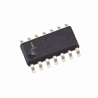
X40431S14I-B Intersil, X40431S14I-B Datasheet - Page 14

X40431S14I-B
Manufacturer Part Number
X40431S14I-B
Description
IC VOLT MON TRPL EEPROM 14-SOIC
Manufacturer
Intersil
Type
Multi-Voltage Supervisorr
Datasheet
1.X40430S14Z-A.pdf
(26 pages)
Specifications of X40431S14I-B
Number Of Voltages Monitored
3
Output
Open Drain or Open Collector
Reset
Active Low
Reset Timeout
Adjustable/Selectable
Voltage - Threshold
1.7V, 2.6V, 4.4V
Operating Temperature
-40°C ~ 85°C
Mounting Type
Surface Mount
Package / Case
14-SOIC (3.9mm Width), 14-SOL
Lead Free Status / RoHS Status
Contains lead / RoHS non-compliant
Available stocks
Company
Part Number
Manufacturer
Quantity
Price
Company:
Part Number:
X40431S14I-B
Manufacturer:
Intersil
Quantity:
100
Page Write
The device is capable of a page write operation. It is
initiated in the same manner as the byte write opera-
tion; but instead of terminating the write cycle after the
first data byte is transferred, the master can transmit
an unlimited number of 8-bit bytes. After the receipt of
each byte, the device will respond with an acknowl-
edge, and the address is internally incremented by
one. The page address remains constant. When the
counter reaches the end of the page, it “rolls over” and
goes back to ‘0’ on the same page.
This means that the master can write 16 bytes to the
page starting at any location on that page. If the mas-
ter begins writing at location 10, and loads 12 bytes,
then the first 6 bytes are written to locations 10
through 15, and the last 6 bytes are written to locations
0 through 5. Afterwards, the address counter would
point to location 6 of the page that was just written. If
the master supplies more than 16 bytes of data, then
new data overwrites the previous data, one byte at a
time.
The master terminates the Data Byte loading by issuing
a stop condition, which causes the device to begin the
nonvolatile write cycle. As with the byte write operation,
all inputs are disabled until completion of the internal
write cycle. See Figure 11 for the address, acknowl-
edge, and data transfer sequence.
Figure 11. Page Write Operation
Figure 12. Writing 12 bytes to a 16-byte page starting at location 10.
Signals from
Signals from
the Master
the Slave
SDA Bus
7 Bytes
address
14
= 6
S
a
t
r
t
1 0 1 0
Address
Slave
X40430, X40431, X40434, X40435
0
address pointer
ends here
Addr = 7
0
0
A
C
K
Address
Byte
Stops and Write Modes
Stop conditions that terminate write operations must
be sent by the master after sending at least 1 full data
byte plus the subsequent ACK signal. If a stop is
issued in the middle of a data byte, or before 1 full
data byte plus its associated ACK is sent, then the
device will reset itself without performing the write. The
contents of the array will not be effected.
Acknowledge Polling
can be used to take advantage of the typical 5ms write
cycle time. Once the stop condition is issued to indi-
cate the end of the master’s byte load operation, the
device initiates the internal high voltage cycle.
Acknowledge polling can be initiated immediately. To
do this, the master issues a start condition followed by
the Slave Address Byte for a write or read operation. If
the device is still busy with the high voltage cycle then
no ACK will be returned. If the device has completed
the write operation, an ACK will be returned and the
host can then proceed with the read or write operation.
See Figure 13.
Serial Read Operations
Read operations are initiated in the same manner as
write operations with the exception that the R/W bit of
the Slave Address Byte is set to one. There are three
basic read operations: Current Address Reads, Ran-
dom Reads, and Sequential Reads.
address
The disabling of the inputs during high voltage cycles
A
C
K
10
Data
(1)
(1 ≤ n ≤ 16)
C
A
K
5 Bytes
Data
address
(n)
n-1
A
C
K
S
o
p
t
May 24, 2006
FN8251.1


