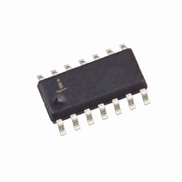
X40431S14-B Intersil, X40431S14-B Datasheet - Page 16

X40431S14-B
Manufacturer Part Number
X40431S14-B
Description
IC VOLT MON TRPL EEPROM 14-SOIC
Manufacturer
Intersil
Type
Multi-Voltage Supervisorr
Datasheet
1.X40430S14Z-A.pdf
(26 pages)
Specifications of X40431S14-B
Number Of Voltages Monitored
3
Output
Open Drain or Open Collector
Reset
Active Low
Reset Timeout
Adjustable/Selectable
Voltage - Threshold
1.7V, 2.6V, 4.4V
Operating Temperature
0°C ~ 70°C
Mounting Type
Surface Mount
Package / Case
14-SOIC (3.9mm Width), 14-SOL
Lead Free Status / RoHS Status
Contains lead / RoHS non-compliant
Available stocks
Company
Part Number
Manufacturer
Quantity
Price
Company:
Part Number:
X40431S14-B
Manufacturer:
Intersil
Quantity:
100
SERIAL DEVICE ADDRESSING
Memory Address Map
CR, Control Register, CR7: CR0
Address: 1FF
FDR, Fault DetectionRegister, FDR7: FDR0
Address: 0FF
General Purpose Memory Organization, A8:A0
Address: 000h to 1FFh
General Purpose Memory Array Configuration
Slave Address Byte
Following a start condition, the master must output a
Slave Address Byte. This byte consists of several parts:
– a device type identifier that is always ‘101x’. Where
– next two bits are ‘0’.
– next bit that becomes the MSB of the address.
Figure 14. X40430, X40431, X40434, X40435
Addressing
Figure 15. Current Address Read Sequence
.
Memory Address
General Purpose Memory
Control Register
Fault Detection Register
General Purpose Memory
Control Register
Fault Detection Register
x = 0 is for Array, x = 1 is for Control Register or
Fault Detection Register.
A8:A0
0FFh
1FFh
000h
100h
hex
hex
Lower 256 bytes
Upper 256 bytes
Word Address
Slave Byte
A7
1
1
1
1
1
16
A6 A5 A4
0
0
0
1
1
Signals from
Signals from
the Master
1
1
1
1
1
the Slave
SDA Bus
0
1
1
1
1
Block Protect Option
X40430, X40431, X40434, X40435
0
0
0
A3 A2
1
1
0
0
0
1
1
S
a
t
r
t
A8 R/W
1
0
A1 A0
1 0 1 0
1
1
R/W
R/W
Address
1
1
Slave
0
0
1
– last bit of the slave command byte is a R/W bit. The
Word Address
The word address is either supplied by the master or
obtained from an internal counter. The internal counter
is undefined on a power-up condition.
Operational Notes
The device powers-up in the following state:
– The device is in the low power standby state.
– The WEL bit is set to ‘0’. In this state it is not possi-
– SDA pin is the input mode.
– RESET/RESET Signal is active for
Data Protection
The following circuitry has been included to prevent
inadvertent writes:
– The WEL bit must be set to allow write operations.
– The proper clock count and bit sequence is required
– A three step sequence is required before writing into
– The WP pin, when held HIGH, prevents all writes to
A
C
K
R/W bit of the Slave Address Byte defines the oper-
ation to be performed. When the R/W bit is a one,
then a read operation is selected. A zero selects a
write operation.
ble to write to the device.
prior to the stop bit in order to start a nonvolatile
write cycle.
the Control Register to change Watchdog Timer or
Block Lock settings.
the array and all the Register.
Data
S
o
p
t
t
PURST
.
May 24, 2006
FN8251.1


