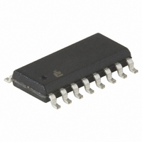
X40235S16I-AT1 Intersil, X40235S16I-AT1 Datasheet - Page 19

X40235S16I-AT1
Manufacturer Part Number
X40235S16I-AT1
Description
IC VOLTAGE MON TRPL EE 16-SOIC
Manufacturer
Intersil
Type
Multi-Voltage Supervisorr
Datasheet
1.X40231S16I-A.pdf
(36 pages)
Specifications of X40235S16I-AT1
Number Of Voltages Monitored
3
Output
Open Drain, Open Drain
Reset
Active High/Active Low
Reset Timeout
Adjustable/Selectable
Voltage - Threshold
1.75V, 2.2V, 2.95V
Operating Temperature
-40°C ~ 85°C
Mounting Type
Surface Mount
Package / Case
16-SOIC (0.300", 7.5mm Width)
Lead Free Status / RoHS Status
Contains lead / RoHS non-compliant
When the Block Lock bits of the CR register are set to
something other than BL1 = 0 and BL0 = 0, then the
“wiper position” of the DCPs cannot be changed - i.e.
DCP write operations cannot be conducted:
The factory default setting for these bits are BL1 = 0,
BL0 = 0.
IMPORTANT NOTE: If the Write Protect (WP) pin of
the X4023x is active (HIGH), then all nonvolatile write
operations to both the EEPROM memory and DCPs
are inhibited, irrespective of the Block Lock bit settings
(See "WP: Write Protection Pin").
PUP1, PUP0: Power-on Reset bits – (Nonvolatile)
Applying voltage to V
circuit which holds RESET output HIGH, until the sup-
ply voltage stabilizes above the V
period of time, t
The Power-on Reset bits, PUP1 and PUP0 of the CR
register determine the t
on Reset circuitry (See "VOLTAGE MONITORING
FUNCTIONS"). These bits of the CR register are non-
volatile, and therefore power-up to the last written
state.
The nominal Power-on Reset delay time can be
selected from the following table, by writing the appro-
priate bits to the CR register:
BL1
SCL
SDA
0
0
1
1
S
T
A
R
T
BL0
0
1
0
1
1
SLAVE ADDRESS BYTE
0
PURST
DCP Write Operation Permissible
1
CC
(See Figure 30).
0
PURST
activates the Power-on Reset
0
19
YES (Default)
1
Figure 18. CR Register Write Command Sequence
delay time of the Power-
X40231, X40233, X40235, X40237, X40239
NO
NO
NO
0
TRIP1
R/W A
threshold for a
C
K
1
1
ADDRESS BYTE
1
1
1
1
The default for these bits are PUP1 = 0, PUP0 = 1.
V2FS, V3FS: Voltage Monitor Status Bits (Volatile)
Bits V2FS and V3FS of the CR register are latched,
volatile flag bits which indicate the status of the Volt-
age Monitor reset output pins V2FAIL and V3FAIL.
At power-up the VxFS (x=2,3) bits default to the value
“0”. These bits can be set to a “1” by writing the appro-
priate value to the CR register. To provide consistency
between the VxFAIL and V
the V
sponding VxFAIL output is HIGH.
Once the VxFS bits have been set to “1”, they will be
reset to “0” if:
—The device is powered down, then back up,
—The corresponding V
CR Register Write Operation
The CR register is accessed using the Slave Address
set to 1010010 (Refer to Figure 4). Following the
Slave Address Byte, access to the CR register
requires an Address Byte which must be set to FFh.
Only one data byte is allowed to be written for each
CR register Write operation. The user must issue a
STOP, after sending this byte to the register, to initiate
the nonvolatile cycle that stores the BP1, BP0, PUP1
and PUP0 bits. The X4023x will not ACKNOWLEDGE
any data bytes written after the first byte is entered
(Refer to Figure 18).
PUP1
1
0
0
1
1
xFS
1
bits can only be set to a “1” when the corre-
PUP0
A
C
K
0
1
0
1
CS7 CS6 CS5 CS4 CS3 CS2 CS1 CS0
CR REGISTER DATA IN
Power-on Reset delay (t
xFAIL
output becomes LOW.
xFS
100ms (Default)
however, the status of
200ms
300ms
50ms
PURESET
A
C
K
April 11, 2005
S
T
O
P
FN8115.0
)


