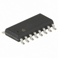
X40233S16I-B Intersil, X40233S16I-B Datasheet - Page 20

X40233S16I-B
Manufacturer Part Number
X40233S16I-B
Description
IC VOLTAGE MON TRPL EE 16-SOIC
Manufacturer
Intersil
Type
Multi-Voltage Supervisorr
Datasheet
1.X40231S16I-A.pdf
(36 pages)
Specifications of X40233S16I-B
Number Of Voltages Monitored
3
Output
Open Drain, Open Drain
Reset
Active High/Active Low
Reset Timeout
Adjustable/Selectable
Voltage - Threshold
1.75V, 2.95V, 4.45V
Operating Temperature
-40°C ~ 85°C
Mounting Type
Surface Mount
Package / Case
16-SOIC (0.300", 7.5mm Width)
Lead Free Status / RoHS Status
Contains lead / RoHS non-compliant
Available stocks
Company
Part Number
Manufacturer
Quantity
Price
Company:
Part Number:
X40233S16I-B
Manufacturer:
Intersil
Quantity:
100
Prior to writing to the CR register, the WEL and RWEL
bits must be set using a two step process, with the
whole sequence requiring 3 steps
—Write a 02H to the CR Register to set the Write Enable
—Write a 06H to the CR Register to set the Register
—Write a one byte value to the CR Register that has all
For example, a sequence of writes to the device CR
register consisting of [02H, 06H, 02H] will reset all of
the nonvolatile bits in the CR Register to “0”.
It should be noted that a write to any nonvolatile bit of
CR register will be ignored if the Write Protect pin of
the X4023x is active (HIGH) (See "WP: Write Protec-
tion Pin").
CR (Control) Register Read Operation
The contents of the CR Register can be read at any
time by performing a random read (See Figure 18).
Using the Slave Address Byte set to 10100101, and
an Address Byte of FFh. Only one byte is read by each
register read operation. The X4023x resets itself after
the first byte is read. The master should supply a
STOP condition to be consistent with the bus protocol.
After setting the WEL and / or the RWEL bit(s) to a “1”,
a CR register read operation may o
rupting a proceeding CR register write operation.
Latch (WEL). This is a volatile operation, so there is no
delay after the write. (Operation preceded by a START
and ended with a STOP).
Write Enable Latch (RWEL) AND the WEL bit. This is
also a volatile cycle. The zeros in the data byte are
required. (Operation preceded by a START and ended
with a STOP).
the bits set to the desired state. The CR register can
be represented as qxyst01r in binary, where xy are the
Voltage Monitor Output Status (V2FS and V3FS) bits,
st are the Block Lock Protection (BL1 and BL0) bits,
and qr are the Power-on Reset delay time (t
control bits (PUP1 - PUP0). This operation is pro-
ceeded by a START and ended with a STOP bit. Since
this is a nonvolatile write cycle, it will typically take 5ms
to complete. The RWEL bit is reset by this cycle and
the sequence must be repeated to change the nonvol-
atile bits again. If bit 2 is set to ‘1’ in this third step (qxys
t11r) then the RWEL bit is set, but the V2FS, V3FS,
PUP1, PUP0, BL1 and BL0 bits remain unchanged.
Writing a second byte to the control register is not
allowed. Doing so aborts the write operation and the
X4023x does not return an ACKNOWLEDGE.
20
X40231, X40233, X40235, X40237, X40239
CC
ur, without inter-
PURST
)
DATA PROTECTION
There are a number of levels of data protection fea-
tures designed into the X4023x. Any write to the
device first requires setting of the WEL bit in the CR
register. A write to the CR register itself, further
requires the setting of the RWEL bit. Block Lock pro-
tection of the device enables the user to inhibit writes
to certain regions of the EEPROM memory, as well as
to all the DCPs. One further level of data protection in
the X4023x, is incorporated in the form of the Write
Protection pin.
WP: Write Protection Pin
When the Write Protection (WP) pin is active (HIGH), it
disables nonvolatile write operations to the X4023x.
The table below (X4023x Write Permission Status)
summarizes the effect of the WP pin (and Block Lock),
on the write permission status of the device.
Additional Data Protection Features
In addition to the preceding features, the X4023x also
incorporates the following data protection functionality:
—The proper clock count and data bit sequence is
VOLTAGE MONITORING FUNCTIONS
V
The X4023x monitors the supply voltage and drives the
RESET output HIGH (using an external “pull up” resis-
tor) if V
output will remain HIGH until V
minimum time of t
is driven to a LOW state. See Figure 30.
For the Power-on / Low Voltage Reset function of the
X4023x, the RESET output may be driven HIGH down
to a V
ture of the X4023x, is that the value of t
selected in software via the CR register (See “PUP1,
PUP0: Power-on Reset bits – (Nonvolatile)” on
page 19.).
It is recommended to stop communication to the
device while RESET is HIGH. Also, setting the Manual
Reset (MR) pin HIGH overrides the Power-on / Low
Voltage circuitry and forces the RESET output pin
HIGH (See "MR: Manual Reset").
CC
required prior to the STOP bit in order to start a nonvol-
atile write cycle.
Monitoring
CC
CC
of 1V (V
is lower than V
PURST
RVALID
. After this time, the RESET pin
). See Figure 30. Another fea-
TRIP1
CC
threshold. The RESET
exceeds V
PURST
TRIP1
April 11, 2005
may be
FN8115.0
for a


