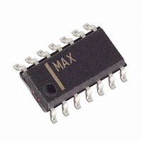
MAX8215CSD+ Maxim Integrated Products, MAX8215CSD+ Datasheet - Page 9

MAX8215CSD+
Manufacturer Part Number
MAX8215CSD+
Description
IC MONITOR VOLT MPU 14-SOIC
Manufacturer
Maxim Integrated Products
Type
Multi-Voltage Supervisorr
Datasheet
1.MAX8216CSD.pdf
(12 pages)
Specifications of MAX8215CSD+
Number Of Voltages Monitored
5
Output
Open Drain or Open Collector
Reset Timeout
20 µs Typical Propagation Delay
Voltage - Threshold
±5V, ±12V, Adj
Operating Temperature
0°C ~ 70°C
Mounting Type
Surface Mount
Package / Case
14-SOIC (3.9mm Width), 14-SOL
Monitored Voltage
- 12 V or - 5 V or 5 V or 12 V
Undervoltage Threshold
4.521 V or 10.431 V or - 10.431 V or - 4.348 V
Overvoltage Threshold
4 V or 10.749 V or - 10.749 V or - 4.482 V
Manual Reset
No
Watchdog
No
Battery Backup Switching
No
Power-up Reset Delay (typ)
85 ms to 300 ms
Supply Voltage (max)
11 V
Supply Voltage (min)
2.7 V
Supply Current (typ)
250 uA
Maximum Power Dissipation
667 mW
Mounting Style
SMD/SMT
Maximum Operating Temperature
+ 70 C
Chip Enable Signals
No
Minimum Operating Temperature
0 C
Output Type
Open Drain
Power Fail Detection
No
Lead Free Status / RoHS Status
Lead free / RoHS Compliant
Reset
-
Lead Free Status / Rohs Status
Lead free / RoHS Compliant
Figure 7. Microprocessor Reset Circuit Monitoring Its Own
Supply Voltage
absolute maximum ratings have no effect on the refer-
ence. Within the absolute maximum ratings, the DIN
input has no effect on the reference.
In high-noise environments where the voltage connected
to V
“bounce,” causing false comparator outputs. Eliminate
this problem using Figure 8’s RC bypass network.
Although bypassing the reference may appear to help,
Figure 8’s solution is recommended; bypassing the ref-
erence reduces its voltage change, but doing so caus-
es a time delay prior to the reference voltage returning
to its correct level.
Although hysteresis is built into the auxiliary comparator,
output oscillation problems are still possible. Oscillation
can occur when a comparator’s output couples back to
its inverting input through stray board capacitance.
Make sure the board trace leading from the comparator
output does not pass near its inverting input (or vice
versa). Also, reducing the resistance connected to DIN
reduces its susceptibility to picking up output signals. In
+V
S
DD
Power-Supply Bypassing and Grounding
may change abruptly, the reference voltage may
Eliminating Output Oscillation when
1 F
3
7
2
DIN
GND
+5V
Using the Auxiliary Comparator
_______________________________________________________________________________________
MAX8215
MAX8216
0.1 F
PGND
8
DOUT
OUT1
V
DD
13
9
14
1k
Microprocessor Voltage Monitors
+5V
680k
680k
±5V, ±12V (±15V) Dedicated
RESET
most cases, using input resistor values on the order of
100k
values increases the supply current, another approach
is to bypass the input resistors as shown in Figure 9,
although this slows the circuit’s response. When much
larger valued input resistors are used, high valued resis-
tors on the output should be used.
When DOUT is required to sink larger currents (i.e.,
when smaller pull-up resistor values are used), oscilla-
tion problems are more likely to occur. To minimize
power consumption and to optimize stability, use the
largest value pull-up resistor feasible for the output
drive required. When lower pull-up resistor values are
used, lower values for the resistors connected to the
inputs can help alleviate oscillation problems.
Figure 8. Alternate Bypass Scheme
Figure 9. Alternative Means for Reducing Impedance Level
Seen at DIN
V
IN
creates no problem. Since using lower resistor
0.1 F
V+
7
MAX8215
MAX8216
1k
14
DIN
V
DD
MAX8215
MAX8216
OUT1
13
DOUT
9
9


