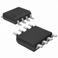
MAX817LCSA Maxim Integrated Products, MAX817LCSA Datasheet - Page 4

MAX817LCSA
Manufacturer Part Number
MAX817LCSA
Description
IC MPU SUPERVISORY CIRCUIT 8SOIC
Manufacturer
Maxim Integrated Products
Type
Battery Backup Circuitr
Datasheet
1.MAX819LCSA.pdf
(16 pages)
Specifications of MAX817LCSA
Number Of Voltages Monitored
1
Output
Push-Pull, Totem Pole
Reset
Active Low
Reset Timeout
140 ms Minimum
Voltage - Threshold
4.65V
Operating Temperature
0°C ~ 70°C
Mounting Type
Surface Mount
Package / Case
8-SOIC (3.9mm Width)
Lead Free Status / RoHS Status
Contains lead / RoHS non-compliant
Other names
Q1785362
Available stocks
Company
Part Number
Manufacturer
Quantity
Price
Part Number:
MAX817LCSA
Manufacturer:
MAXIM/美信
Quantity:
20 000
Part Number:
MAX817LCSA+
Manufacturer:
MAXIM/美信
Quantity:
20 000
Company:
Part Number:
MAX817LCSA+T
Manufacturer:
CYPRESS
Quantity:
6 220
+5V Microprocessor Supervisory Circuits
ELECTRICAL CHARACTERISTICS (continued)
(V
noted. Typical values are at T
4
Note 2: Either V
Note 3: “-” = battery-charging current, “+” = battery-discharging current.
Note 4: WDI is internally serviced within the watchdog timeout period if WDI is left unconnected.
Note 5: WDI input is designed to be driven by a three-stated output device. To float WDI, the “high-impedance mode” of the output
Note 6: The chip-enable resistance is tested with V
Note 7: The chip-enable propagation delay is measured from the 50% point at CE IN to the 50% point at CE OUT.
CHIP-ENABLE GATING (MAX818 only)
CE IN Leakage Current
CE IN to CE OUT Resistance
(Note 6)
CE OUT Short-Circuit Current
(Reset Active)
CE IN to CE OUT Propagation
Delay (Note 7)
CE OUT Output
CE OUT Input Threshold
RESET to CE OUT Delay
CC
_______________________________________________________________________________________
= +4.75V to +5.5V for MAX81_L, V
device must have a maximum leakage current of 10µA and a maximum output capacitance of 200pF. The output device
must also be able to source and sink at least 200µA when active.
V
PARAMETER
C E IN
= V
CC
C E OUT
or V
BATT
= V
A
can go to 0V if the other is greater than 2.0V.
= +25°C.)
CC
SYMBOL
/2.
V
V
V
OH
IH
IL
CC
= +4.5V to +5.5V for MAX81_M, V
Disable mode
Enable mode
Disable mode, CE OUT = 0V
50 source impedance driver, C
I
I
V
Power-down
OUT
OUT
CC
= 5V
CC
= -100µA, V
= -1µA, V
= +4.75V for the MAX818L and V
CC
CONDITIONS
CC
= 0V, V
= 0V
BATT
= 2.8V
LOAD
BATT
= 50pF
= 2.8V, T
CC
= +4.5V for the MAX818M.
V
A
CC
MIN
0.1
2.7
3.5
= T
- 1V
MIN
±0.005
to T
TYP
0.75
40
15
3
MAX
, unless otherwise
MAX
150
2.0
0.8
±1
8
UNITS
mA
µA
ns
µs
V
V


