DS1706ESA/T&R Maxim Integrated Products, DS1706ESA/T&R Datasheet - Page 2

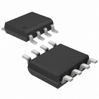
DS1706ESA/T&R
Manufacturer Part Number
DS1706ESA/T&R
Description
IC MICROMONITOR 5V 10% 8-SOIC
Manufacturer
Maxim Integrated Products
Series
MicroMonitor™r
Type
Simple Reset/Power-On Resetr
Datasheet
1.DS1706SESA.pdf
(12 pages)
Specifications of DS1706ESA/T&R
Number Of Voltages Monitored
1
Output
Push-Pull, Totem Pole
Reset
Active Low
Reset Timeout
130 ms Minimum
Voltage - Threshold
4.4V
Operating Temperature
-40°C ~ 85°C
Mounting Type
Surface Mount
Package / Case
8-SOIC (3.9mm Width)
Monitored Voltage
3.3 V, 5 V
Undervoltage Threshold
4.25 V
Overvoltage Threshold
4.5 V
Output Type
Active Low, Push-Pull
Manual Reset
Resettable
Watchdog
Watchdog
Battery Backup Switching
No Backup
Power-up Reset Delay (typ)
285 ms
Supply Voltage (max)
5.5 V
Supply Voltage (min)
1.2 V
Supply Current (typ)
60 uA
Maximum Operating Temperature
+ 85 C
Mounting Style
SMD/SMT
Minimum Operating Temperature
- 40 C
Power Fail Detection
Yes
Lead Free Status / RoHS Status
Contains lead / RoHS non-compliant
Available stocks
Company
Part Number
Manufacturer
Quantity
Price
Part Number:
DS1706ESA/T&RDS1706ESA/T&R
Manufacturer:
MAXIM/美信
Quantity:
20 000
the reset to an active state. When V
active state for a minimum of 130 ms to allow the power supply and processor to stabilize.
The second function the DS1705/DS1706 performs is pushbutton reset control. The DS1705/DS1706
debounces the pushbutton input and guarantees an active reset pulse width of 130 ms minimum.
The third function is a watchdog timer. The DS1705/DS1706 has an internal timer that forces the WDS
output signal to the active state if the strobe input is not driven low prior to time-out.
OPERATION
Power Monitor
The DS1705/DS1706 detects out-of-tolerance power supply conditions and warns a processor-based
system of impending power failure. When V
outputs the
processing is stopped at the last possible moment of valid V
active for a minimum of 130 ms to allow the power supply and processor to stabilize.
Pushbutton Reset
The DS1705/DS1706 provides an input pin for direct connection to a pushbutton reset (see Figure 2). The
pushbutton reset input requires an active low signal. Internally, this input is debounced and timed such
that a
as the pushbutton reset input is released from the low level. The pushbutton can be initiated by connecting
the
Non-Maskable Interrupt
The DS1705/DS1706 generates a non-maskable interrupt (
precision comparator monitors the voltage level at the IN pin relative to an on-chip reference generated
by an internal band gap. The IN pin is a high impedance input allowing for a user-defined sense point. An
external resistor voltage divider network (Figure 5) is used to interface with high voltage signals. This
sense point may be derived from a regulated supply or from a higher DC voltage level closer to the main
system power input. Since the IN trip point V
determined by the equation as shown in Figure 5. Proper operation of the DS1705/DS1706 requires that
the voltage at the IN pin be limited to V
monitored (V
to select a value for R2 high enough to keep power consumption low, and solve for R1. The flexibility of
the IN input pin allows for detection of power loss at the earliest point in a power supply system,
maximizing the amount of time for system shutdown between
When the supply being monitored decays to the voltage sense point, the DS1705/DS1706 pulses the
output to the active state for a minimum 200 s. The
hysteresis of 100 V. The supply must be below the voltage sense point for approximately 5 s before a
low
preventing false interrupts. During a power-up, any detected IN pin levels below V
are disabled from generating an interrupt until V
will not be initiated until V
Connecting
out-of-tolerance condition occurred in a monitored supply. An example is shown in Figure 3.
WDS
NMI
RST
or
will be generated. In this way, power supply noise is removed from the monitoring function,
(or RST) signal of at least 130 ms minimum will be generated. The 130 ms delay commences
RST
NMI
NMI
MAX
) can also be derived as shown in Figure 5. A simple approach to solving the equation is
(or RST) signal.
outputs to the
to
PBRST
CC
would allow non-maskable interrupt to generate an automatic reset when an
reaches V
PBRST
RST
CC
returns to an in-tolerance condition, the reset signal is kept in the
CCTP
CC
input as shown in Figure 3.
(or RST) is an excellent control signal for a microprocessor, as
. Therefore, the maximum allowable voltage at the supply being
.
CC
TP
falls below the minimum V
CC
2 of 12
is 1.25 volts, the proper values for R1 and R2 can be
rises to V
NMI
power-fail detection circuitry also has built-in
NMI
NMI
CCTP
CC
) for early warning of a power failure. A
. On power-up,
. As a result, any potential
and
RST
(or RST).
CC
tolerance, a comparator
RST
TP
(or RST) are kept
by the comparator
NMI
pulse
NMI


