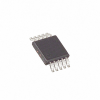
DS4510U-10 Maxim Integrated Products, DS4510U-10 Datasheet - Page 8

DS4510U-10
Manufacturer Part Number
DS4510U-10
Description
IC SUPERVISOR W/NV MEM 10-USOP
Manufacturer
Maxim Integrated Products
Type
Simple Reset/Power-On Resetr
Datasheet
1.DS4510U-10.pdf
(12 pages)
Specifications of DS4510U-10
Number Of Voltages Monitored
1
Output
Open Drain or Open Collector
Reset
Active Low
Reset Timeout
Adjustable/Selectable
Voltage - Threshold
4.375V
Operating Temperature
-40°C ~ 85°C
Mounting Type
Surface Mount
Package / Case
10-MSOP, Micro10™, 10-uMAX, 10-uSOP
Undervoltage Threshold
4.25 V
Overvoltage Threshold
4.49 V
Output Type
Active Low, Open Drain
Manual Reset
Not Resettable
Watchdog
No Watchdog
Battery Backup Switching
No Backup
Power-up Reset Delay (typ)
1100 ms
Supply Voltage (max)
5.5 V
Supply Voltage (min)
2.7 V
Maximum Operating Temperature
+ 85 C
Mounting Style
SMD/SMT
Minimum Operating Temperature
- 40 C
Power Fail Detection
No
Lead Free Status / RoHS Status
Contains lead / RoHS non-compliant
CPU Supervisor with Nonvolatile Memory and
Programmable I/O
Figure 4. Register Bit Names
The following terminology is commonly used to
describe I
Master Device: The master device controls the slave
devices on the bus. The master device generates SCL
clock pulses, start, and stop conditions.
Slave Devices: Slave devices send and receive data
at the master’s request.
Bus Idle or Not Busy: Time between stop and start
conditions when both SDA and SCL are inactive and in
their logic-high states. When the bus is idle it often initi-
ates a low-power mode for slave devices.
Start Condition: A start condition is generated by the
master to initiate a new data transfer with a slave.
Transitioning SDA from high to low while SCL remains
high generates a start condition. See the timing dia-
gram for applicable timing.
Stop Condition: A stop condition is generated by the
master to end a data transfer with a slave. Transitioning
8
REGISTER
User SRAM
RST Delay
I/O Status
Reserved
User SEE
User SEE
EEPROM
Control
Control
Control
Control
Enable
NAME
Config
Pullup
User
I/O3
I/O2
I/O1
I/O0
_____________________________________________________________________
2
C data transfers.
LOCATION
REGISTER
(HEX)
00-3F
40-EF
FA-FF
F0
F1
F2
F3
F4
F5
F6
F7
F8
F9
SRAM
ready
Bit 7
SEE
SEE
SEE
SEE
SEE
SEE
SEE
SEE
n/a
EE
0
trip point
SRAM
Bit 6
SEE
SEE
SEE
SEE
SEE
SEE
SEE
SEE
n/a
EE
I
0
2
C Definitions
status
SRAM
reset
SEE
SEE
SEE
SEE
SEE
SEE
SEE
SEE
Bit5
n/a
EE
0
REGISTER BIT NAMES
SRAM
Bit 4
SEE
SEE
SEE
SEE
SEE
SEE
SEE
SEE
SEE
n/a
EE
0
SDA from low to high while SCL remains high gener-
ates a stop condition. See the I
applicable timing.
Repeated Start Condition: The master can use a
repeated start condition at the end of one data transfer
to indicate that it will immediately initiate a new data
transfer following the current one. Repeated starts are
commonly used during read operations to identify a
specific memory address to begin a data transfer. A
repeated start condition is issued identically to a nor-
mal start condition. See the I
applicable timing.
Bit Write: Transitions of SDA must occur during the low
state of SCL. The data on SDA must remain valid and
unchanged during the entire high pulse of SCL (see
Figure
Data is shifted into the device during the rising edge of
the SCL.
Bit Read: At the end a write operation, the master must
release the SDA bus line for the proper amount of setup
SWRST
pullup
Status
SRAM
Bit 3
I/O3
SEE
SEE
SEE
SEE
SEE
SEE
SEE
I/O3
n/a
EE
5) plus the setup and hold-time requirements.
pullup
Status
SRAM
Bit 2
I/O2
I/O2
SEE
SEE
SEE
SEE
SEE
SEE
SEE
n/a
EE
0
pullup
Status
SRAM
Bit 1
I/O1
I/O1
TD1
SEE
SEE
SEE
SEE
SEE
SEE
n/a
EE
0
2
C Timing Diagram for
2
pullup
Status
SRAM
C Timing Diagram for
Bit 0
I/O0
TD0
SEE
SEE
I/O3
I/O2
I/O1
I/O0
I/O0
n/a
EE
0
FACTORY OR
POWER-ON
DEFAULT
XXX00000
00000000
00000000
00000011
00000000
00000000
00000001
00000001
00000001
00000001
00000000
(BIN)
n/a
n/a


