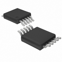
LTC2900-1CMS Linear Technology, LTC2900-1CMS Datasheet - Page 3

LTC2900-1CMS
Manufacturer Part Number
LTC2900-1CMS
Description
IC MON SUPP QUAD OPEN DRN 10MSOP
Manufacturer
Linear Technology
Type
Multi-Voltage Supervisorr
Datasheet
1.LTC2900-2CMSPBF.pdf
(16 pages)
Specifications of LTC2900-1CMS
Number Of Voltages Monitored
4
Output
Open Drain or Open Collector
Reset
Active Low
Reset Timeout
5 ms Minimum
Voltage - Threshold
16 Selectable Threshold Combinations
Operating Temperature
0°C ~ 70°C
Mounting Type
Surface Mount
Package / Case
10-MSOP, Micro10™, 10-uMAX, 10-uSOP
Lead Free Status / RoHS Status
Contains lead / RoHS non-compliant
Available stocks
Company
Part Number
Manufacturer
Quantity
Price
Company:
Part Number:
LTC2900-1CMS
Manufacturer:
LT
Quantity:
5 321
Company:
Part Number:
LTC2900-1CMS
Manufacturer:
LT
Quantity:
10 000
Part Number:
LTC2900-1CMS
Manufacturer:
LINEAR/凌特
Quantity:
20 000
Company:
Part Number:
LTC2900-1CMS#PBF
Manufacturer:
LINEAR
Quantity:
1
Company:
Part Number:
LTC2900-1CMS#TRPBF
Manufacturer:
WDC
Quantity:
6 218
Part Number:
LTC2900-1CMS#TRPBF
Manufacturer:
LT/凌特
Quantity:
20 000
Company:
Part Number:
LTC2900-1CMS(LTYJ)
Manufacturer:
ST
Quantity:
9 004
Part Number:
LTC2900-1CMS(LTYJ)
Manufacturer:
LT/凌特
Quantity:
20 000
Part Number:
LTC2900-1CMS10
Manufacturer:
LINEAR/凌特
Quantity:
20 000
Part Number:
LTC2900-1CMS8
Manufacturer:
LINEAR/凌特
Quantity:
20 000
ELECTRICAL CHARACTERISTICS
temperature range, otherwise specifications are at T
SYMBOL
I
I
I
I
I
t
t
V
V
Manual Reset Pin
V
V
t
t
I
Note 1: Absolute Maximum Ratings are those values beyond which the life of
a device may be impaired.
Note 2: All currents into pins are positive, all voltages are referenced to GND
unless otherwise noted.
Note 3: The greater of V1, V2 is the internal supply voltage (V
Note 4: Under static no-fault conditions, V1 will necessarily supply quiescent
current. If at any time V2 is larger than V1, V2 must be capable of supplying
TEST CIRCUITS
V2
V3
V4
CRT(UP)
CRT(DN)
RST
UV
PBW
PBD
PBR
OL
OH
IH
IL
V2 Input Current
V3 Input Current
V4 Input Current
CRT Pull-Up Current
CRT Pull-Down Current
Reset Time-Out Period
V
Output Voltage Low RST
Output Voltage High RST (LTC2900-1)
Output Voltage High RST (LTC2900-2)
(Note 6)
PBR Input Threshold High
PBR Input Threshold Low
PBR Input Pulse Width
Manual Reset Propagation Delay
PBR Pull-Up Current
PARAMETER
(Note 5)
X
Undervoltage Detect to RST
Figure 1. RST V
V1
V2
V3
V4
LTC2900-1 RST
2900 F01
OH
Test
I
1 A
SOURCE
A
CONDITIONS
V2 = 3.3V
V3 = 2.5V
V3 = 0.55V (ADJ Mode)
V4 = 1.8V
V4 = 0.55V (ADJ Mode)
V4 = –0.05V (–ADJ Mode)
V
V
C
V
by More Than 1%
I
V3, V4 = 0V; V
I
I
I
I
V
V
V
V
V
SINK
SINK
SINK
SOURCE
SOURCE
CC
= 25 C. V
CRT
CRT
RT
X
CC
CC
CC
CC
PBR
).
Less Than Reset Threshold V
Figure 2. RST V
= 1500pF
= 3.3V to 5.5V
= 3.3V to 5.5V
= 3.3V
= 3.3V, V
= 0V
= 1.3V
= 2.5mA; V1 = 3V, V2 = 3V;
= 100 A; V2 = 1V; V1, V3, V4 = 0V
= 100 A; V1 = 1V; V2, V3, V4 = 0V
V1
V2
V3
V4
= 0V
The
= 1 A
= 200 A
LTC2900-1
CC
PBR
denotes the specifications which apply over the full operating
PG
= 5V, unless otherwise noted. (Note 3)
2900 F02
= 0V
Falling
the quiescent current, programming (transient) current and reference load
current.
Note 5: The RST output pin on the LTC2900-1 has an internal pull-up to V2
of typically 6 A. However, an external pull-up resistor may be used when
faster rise times are required or for V
Note 6: The push-pull RST output pin on the LTC2900-2 is actively pulled up
to V2.
RST
OL
Test
I
2.5mA,
100 A
SINK
RTX
Figure 3. Active Pull-Up
RST V
V1
V2
V3
V4
0.8 • V2
V2 – 1
OH
–1.4
MIN
–15
–15
–15
150
0.4
10
LTC2900-2 RST
5
OH
Test
voltages greater than V2.
2900 F03
0.52
0.34
0.15
0.05
0.05
TYP
–10
150
0.8
0.1
–2
20
7
I
200 A
SOURCE
LTC2900
MAX
–2.6
1.2
0.8
0.4
0.3
0.3
1.6
15
15
15
30
2
9
1
UNITS
3
2900f
ms
nA
nA
nA
ns
A
A
A
A
A
V
V
V
V
V
V
V
A
s
s


