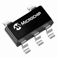
TC53N2202ECTTR Microchip Technology, TC53N2202ECTTR Datasheet - Page 2

TC53N2202ECTTR
Manufacturer Part Number
TC53N2202ECTTR
Description
IC VOLTAGE DETCTR 2.2V SOT23A-5
Manufacturer
Microchip Technology
Type
Simple Reset/Power-On Resetr
Datasheet
1.TC53C2202ECTTR.pdf
(10 pages)
Specifications of TC53N2202ECTTR
Number Of Voltages Monitored
1
Output
Open Drain or Open Collector
Reset
Active Low
Reset Timeout
200 µs Maximum
Voltage - Threshold
2.2V
Operating Temperature
-40°C ~ 85°C
Mounting Type
Surface Mount
Package / Case
SOT-23-5, SC-74A, SOT-25
Monitored Voltage
1.6 V to 6 V
Manual Reset
Not Resettable
Watchdog
No Watchdog
Supply Voltage (max)
10 V
Supply Voltage (min)
1.5 V
Supply Current (typ)
4.2 uA
Maximum Power Dissipation
240 mW
Maximum Operating Temperature
+ 85 C
Mounting Style
SMD/SMT
Minimum Operating Temperature
- 40 C
Lead Free Status / RoHS Status
Lead free / RoHS Compliant
TC53
1.0
Absolute Maximum Ratings*
Input Voltage ........................................................+12V
Output Current .................................................... 50mA
Output Voltage ......................V
Power Dissipation
Operating Temperature Range............. -40°C to +85°C
Storage Temperature Range .............. -40°C to +125°C
TC53 ELECTRICAL SPECIFICATIONS
DS21432C-page 2
Electrical Characteristics: T
V
V
I
V
I
( T
Note
SS
OUT
t
DLY
V
DF
HYS
IN
Symbol
DF
5-Pin SOT-23A ...........................................240mW
OPR
/
1:
2:
3:
V
ELECTRICAL
CHARACTERISTICS
DF
An additional resistor between the V
V
The power consumption during power-start to output being stable (release operation) is 2 A greater than it is after that period
(completion of release operation) because of rush current in the delay circuit.
V
)
DR
T
is the factory-programmed voltage detection threshold.
.
Detect Voltage
Hysteresis Range
Supply Current
Operating Voltage
Output Current
Temperature Characteristics
Delay Time
(V
DR
V
Parameter
OUT
A
Inversion)
= 25°C, unless otherwise specified. Note 1, Note 2.
IN
+ 0.3V to V
IN
pin and the supply voltage may alter the electrical characteristics due to the increasing values of
V
V
SS
DF
T
Min
1.5
x 0.98
—
—
—
—
—
—
—
—
—
—
—
—
—
x 0.02
– 0.3V
V
V
DF
T
-10.0
±100
10.1
11.5
13.0
Typ
±0.5%
0.9
1.0
1.3
1.6
2.0
2.2
7.7
—
—
x 0.05
*Stresses above those listed under "Absolute Maximum
Ratings" may cause permanent damage to the device. These
are stress ratings only and functional operation of the device
at these or any other conditions above those indicated in the
operation sections of the specifications is not implied.
Exposure to Absolute Maximum Rating conditions for
extended periods may affect device reliability.
V
V
DF
T
Max
10.0
x 1.02
2.6
3.0
3.4
3.8
4.2
0.2
—
—
—
—
—
—
—
x 0.08
ppm/°C
Units
msec
mA
V
V
V
A
Note 3
V
V
V
V
V
V
N-ch; V
P-ch; V
(CMOS Output)
IN
IN
IN
IN
IN
DF
2002 Microchip Technology Inc.
= 1.5V
= 2.0V
= 3.0V
= 4.0V
= 5.0V
= 2.1 to 6.0V
DS
DS
Test Conditions
= 2.1V, V
= 0.5V, V
V
V
V
V
IN
IN
IN
IN
IN
IN
= 1.0V
= 2.0V
= 3.0V
= 4.0V
= 5.0V
= 8.0V


