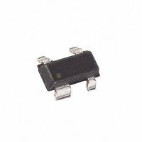
MAX836EUS+T Maxim Integrated Products, MAX836EUS+T Datasheet - Page 4

MAX836EUS+T
Manufacturer Part Number
MAX836EUS+T
Description
IC MONITOR VOLT LP SOT143-4
Manufacturer
Maxim Integrated Products
Type
Simple Reset/Power-On Resetr
Datasheet
1.MAX837EUST.pdf
(7 pages)
Specifications of MAX836EUS+T
Number Of Voltages Monitored
1
Output
Open Drain or Open Collector
Reset
Active Low
Reset Timeout
80 µs Typical Propagation Delay
Voltage - Threshold
Adjustable/Selectable
Operating Temperature
-40°C ~ 85°C
Mounting Type
Surface Mount
Package / Case
SOT-143, SOT-143B, TO-253AA
Manual Reset
Not Resettable
Watchdog
No Watchdog
Supply Voltage (max)
11 V
Supply Voltage (min)
2.5 V
Supply Current (typ)
6.5 uA
Maximum Power Dissipation
320 mW
Maximum Operating Temperature
+ 85 C
Mounting Style
SMD/SMT
Minimum Operating Temperature
- 40 C
Lead Free Status / RoHS Status
Lead free / RoHS Compliant
Other names
MAX836EUS+T
MAX836EUS+TTR
MAX836EUS+TTR
4-Pin Micropower Voltage Monitors
_____________________________Typical Operating Characteristics (continued)
(V
_____________________Pin Description
Figure 1. Programming the Trip Voltage, V
4
CC
PIN
1
2
3
4
_ _ _ _ _ _ _ _ _ _ _ _ _ _ _ _ _ _ _ _ _ _ _ _ _ _ _ _ _ _ _ _ _ _ _ _ _ _ _ _ _ _ _ _ _ _ _ _ _ _ _ _ _ _ _ _ _ _ _ _ _ _ _ _ _ _ _ _ _ _ _ _ _ _ _ _ _ _ _ _ _ _ _ _ _ _ _ _ _ _ _ _ _ _ _ _ _ _ _ _ _ _ _ _ _ _ _ _ _ _ _ _ _ _ _ _ _ _ _ _ _ _ _ _ _ _ _ _ _ _ _ _ _ _ _ _ _ _ _ _ _ _ _ _ _ _ _ _ _ _ _ _ _ _ _ _ _ _ _ _ _ _ _ _ _ _ _ _ _ _ _ _ _ _
V
= +5V, R
TRIP
0.1μF
V
CC
= (1.204)
NAME
GND
OUT
V
NOTE: UNITS ARE OHMS AND VOLTS
IN
LOAD
CC
R1 + R2
R2
160
140
120
100
80
60
40
= 1MΩ, R
-60
1mV/μs
System Ground
System Supply Input
Noninverting Input to the Comparator.
The inverting input connects to the
internal 1.204V bandgap reference.
Open-Drain (MAX836) or
Push-Pull (MAX837) Output
10mV/μs
V
GND
CC
-40
V
CC
FALLING PROPAGATION DELAY
-20
MAX836
PULLUP
vs. TEMPERATURE
R1
TEMPERATURE (°C)
0
FUNCTION
OUT
= 10kΩ (MAX836 only), T
20
IN
40
TRIP
V
TRIP
V
V
V
TRIP
60
V
TRIP
TRIP
= 4.63V
CC
= 4.63V
= 3.0V
= 3.0V
R2
80
R
PULLUP
100
A
= +25°C, unless otherwise noted.)
The MAX836/MAX837 micropower voltage monitors
contain a 1.204V precision bandgap reference and a
comparator (see the Typical Operating Circuit ). The
only difference between the two parts is the structure of
the comparator output driver. The MAX836 has an
open-drain n-channel output driver that can be pulled
up to a voltage higher than V
MAX837’s output is push-pull, and can both source
and sink current.
Two external resistors set the trip voltage, V
V
V
impedance allows large-value resistors without compro-
mising trip-voltage accuracy. To minimize current con-
sumption, select a value for R2 between 500kΩ and
1MΩ, then calculate R1 as follows:
where V
threshold trip voltage (1.204V).
Hysteresis adds noise immunity to the MAX836/MAX837
and prevents repeated triggering when V
threshold trip voltage. Figure 2 shows how to add hys-
teresis to the comparator. The technique is similar for
TRIP
CC
) toggles OUT. The MAX836/MAX837’s high input
is the point at which the applied voltage (typically
1800
1600
1400
1200
1000
800
600
400
200
TRIP
0
2
= desired trip voltage (in volts), V
3
Applications Information
Programming the Trip Voltage
4
R1 = R2
vs. SUPPLY VOLTAGE
OUT RISE/FALL-TIME
5
RISE TIME
MAX837 ONLY
Detailed Description
6
V
CC
7
(V)
⎛
⎜
⎝
8
V
V
TRIP
TH
FALL TIME
CC
9
Adding Hysteresis
10
, but under 11V. The
- 1
⎞
⎟
⎠
11 12
TRIP
IN
is near the
(Figure 1).
TH
=


