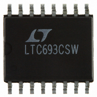
LTC693CSW Linear Technology, LTC693CSW Datasheet - Page 5

LTC693CSW
Manufacturer Part Number
LTC693CSW
Description
IC MPU SUPERVISRY CIRCUIT 16SOIC
Manufacturer
Linear Technology
Type
Simple Reset/Power-On Resetr
Datasheet
1.LTC692CS8PBF.pdf
(20 pages)
Specifications of LTC693CSW
Number Of Voltages Monitored
1
Output
Open Drain or Open Collector
Reset
Active High/Active Low
Reset Timeout
140 ms Minimum
Voltage - Threshold
4.4V
Operating Temperature
0°C ~ 70°C
Mounting Type
Surface Mount
Package / Case
16-SOIC (0.300", 7.5mm Width)
Lead Free Status / RoHS Status
Contains lead / RoHS non-compliant
Other names
LTC693CS
Available stocks
Company
Part Number
Manufacturer
Quantity
Price
Part Number:
LTC693CSW
Manufacturer:
LINEAR/凌特
Quantity:
20 000
Part Number:
LTC693CSW#TRPBF
Manufacturer:
LTNEAR
Quantity:
20 000
ELECTRICAL CHARACTERISTICS
PARAMETER
Oscillator
OSC IN Input Current (Note 7)
OSC SEL Input Pull-Up Current (Note 7)
OSC IN Frequency Range
OSC IN Frequency with External Capacitor
temperature range, otherwise specifi cations are at T
Note 1: Stresses beyond those listed under Absolute Maximum Ratings
may cause permanent damage to the device. Exposure to any Absolute
Maximum Rating condition for extended periods may affect device
reliability and lifetime.
Note 2: All voltage values are with respect to GND.
Note 3: For military temperature range, consult the factory.
Note 4: The output pins of BATT ON, LOW LINE, PFO, WDO, RESET and
RESET have weak internal pull-ups of typically 3μA. However, external
pull-up resistors may be used when higher speed is required.
Note 5: The LTC692/LTC693 have minimum reset active times of 140ms
(200ms typically). The reset active time of the LTC693 can be adjusted
(see Table 2 in Applications Information Section).
CONDITIONS
OSC SEL = 0V
OSC SEL = 0V, C
A
= 25°C. V
OSC
The
= 47pF
l
CC
denotes the specifi cations which apply over the full operating
= full operating range, V
Note 6: The external clock feeding into the circuit passes through the
oscillator before clocking the watchdog timer (see Block Diagram).
Variation in the timeout period is caused by phase errors which occur
when the oscillator divides the external clock by 64. The resulting variation
in the timeout period is 64 clocks plus one clock of jitter.
Note 7: The input pins of CE IN, OSC IN and OSC SEL have weak internal
pull-ups which pull to the supply when the input pins are fl oating.
l
MIN
BATT
0
= 2.8V, unless otherwise noted.
LTC692/LTC693
TYP
±2
5
4
MAX
250
UNITS
0692fb
5
kHz
kHz
μA
μA


