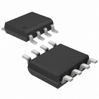
DS1834AS+ Maxim Integrated Products, DS1834AS+ Datasheet - Page 4

DS1834AS+
Manufacturer Part Number
DS1834AS+
Description
IC ECONORST DUAL LO OPN-DR 8SOIC
Manufacturer
Maxim Integrated Products
Series
EconoResetr
Type
Multi-Voltage Supervisorr
Datasheet
1.DS1834AUTR.pdf
(7 pages)
Specifications of DS1834AS+
Number Of Voltages Monitored
2
Output
Open Drain or Open Collector
Reset
Active Low
Reset Timeout
200 ms Minimum
Voltage - Threshold
3.3V, 5V
Operating Temperature
-40°C ~ 85°C
Mounting Type
Surface Mount
Package / Case
8-SOIC (3.9mm Width)
Monitored Voltage
3.3 V or 5 V
Undervoltage Threshold
4.5 V or 2.8 V
Overvoltage Threshold
4.75 V or 2.97 V
Manual Reset
Resettable
Watchdog
No
Battery Backup Switching
No
Power-up Reset Delay (typ)
500 ms
Supply Voltage (max)
5.5 V
Supply Voltage (min)
1.2 V
Supply Current (typ)
50 uA
Mounting Style
SMD/SMT
Maximum Operating Temperature
+ 85 C
Chip Enable Signals
No
Minimum Operating Temperature
- 40 C
Output Type
Active Low or Open Drain
Power Fail Detection
Yes
Lead Free Status / RoHS Status
Lead free / RoHS Compliant
DS1834/A/D
OUTPUT VALID CONDITIONS
All versions of the DS1834 can maintain valid outputs as long as one input remains above 1.2 volts.
However, the
outputs on the DS1834 use a push-pull output structure which can maintain a valid
RST
output below 1.2 volts. To sink current below 1.2 volts a resistor can be connected from
to GND
RST
(see Figure 5). This arrangement will maintain a valid value on the
outputs even if all inputs are at 0
RST
volts. During both power-up and power-down this arrangement will draw current when
is in the high
RST
state. A value of about 100 k =should be adequate to maintain a valid condition.
The DS1834A requires pull-up resistors on the outputs to maintain a valid output. The value of the
resistors is not critical in most cases but must be set low enough to pull the output to a high state. A
common value used is 10 k s (see Figure 6 and Figure 7).
APPLICATION DIAGRAM:
VALID TO 0 VOLTS V
ON THE DS1834 Figure 5
RST
CC
APPLICATION DIAGRAM: DS1834A NMOS OUTPUTS Figure 6
Note: If outputs are pulled-up to different voltages the outputs can not be connected to form a wired
"AND".
APPLICATION DIAGRAM: DS1834A WIRED "AND" OUTPUT Figure 7
4 of 7


