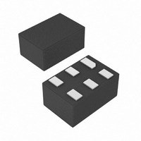
MAX6895PALT+T Maxim Integrated Products, MAX6895PALT+T Datasheet - Page 10

MAX6895PALT+T
Manufacturer Part Number
MAX6895PALT+T
Description
IC SEQUENCE/SUPERVISOR 6UDFN
Manufacturer
Maxim Integrated Products
Type
Sequencerr
Datasheet
1.MAX6896PALTT.pdf
(15 pages)
Specifications of MAX6895PALT+T
Number Of Voltages Monitored
1
Output
Push-Pull, Totem Pole
Reset
Active High
Reset Timeout
Adjustable/Selectable
Voltage - Threshold
Adjustable/Selectable
Operating Temperature
-40°C ~ 125°C
Mounting Type
Surface Mount
Package / Case
6-µDFN
Output Type
Active High, Push-Pull
Manual Reset
Not Resettable
Watchdog
No Watchdog
Battery Backup Switching
No Backup
Supply Voltage (max)
5.5 V
Supply Voltage (min)
1.5 V
Supply Current (typ)
10 uA
Maximum Power Dissipation
167.7 mW
Maximum Operating Temperature
+ 125 C
Mounting Style
SMD/SMT
Minimum Operating Temperature
- 40 C
Power Fail Detection
No
Lead Free Status / RoHS Status
Lead free / RoHS Compliant
Other names
MAX6895PALT+T
MAX6895PALT+TTR
MAX6895PALT+TTR
Ultra-Small, Adjustable
Sequencing/Supervisory Circuits
The MAX6895/MAX6897 offer an active-high enable
input (ENABLE), while the MAX6896/MAX6898/MAX6899
offer an active-low enable input (ENABLE). With V
V
(OUT low) after the adjustable delay time (A versions). For
P version devices, when V
ed, the output asserts after typically 150ns.
The enable input has logic-high and logic-low voltage
thresholds of 1.4V and 0.4V, respectively. For both ver-
sions, when V
high) to force OUT low (OUT high) within 150ns typ.
The MAX6895/MAX6899 offer an active-high, push-pull
output (OUT), and the MAX6896 offers an active-low
push-pull output (OUT). The MAX6897 offers an active-
high open-drain output (OUT), and the MAX6898 offers
an active-low open-drain output (OUT).
Push-pull output devices are referenced to V
drain outputs can be pulled up to 28V.
Figure 7. MAX6899P Timing Diagram
10
TH
ENABLE
, drive ENABLE high (ENABLE low) to force OUT high
V
OUT
______________________________________________________________________________________
CC
IN
Enable Input (ENABLE or ENABLE )
IN
> 0.5V, drive ENABLE low (ENABLE
V
UVLO
IN
> 0.5V and enable is assert-
Output (OUT or OUT )
t
PROPP
CC
IN
. Open-
above
t
DL
The MAX6895–MAX6899 monitor the voltage on IN with
an external resistive divider (see R1 and R2 in the
Typical Operating Circuit ). Connect R1 and R2 as close
to IN as possible. R1 and R2 can have very high values
to minimize current consumption due to low IN leakage
currents (±15nA max). Set R2 to some conveniently
high value (1MΩ, for example) and calculate R1 based
on the desired monitored voltage using the following
formula:
where V
V
IN
is the detector input threshold (0.5V).
t
DELAY
MONITOR
R
Applications Information
1
=
is the desired monitored voltage and
R
2
t
OFF
×
t > t
⎡
⎢
⎣
PW
V
MONITOR
V
IN
Input Threshold
t
PROPP
−
1
⎤
⎥
⎦


