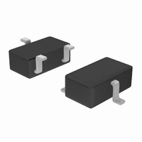
XC61HC1612MR-G Torex Semiconductor Ltd, XC61HC1612MR-G Datasheet - Page 4

XC61HC1612MR-G
Manufacturer Part Number
XC61HC1612MR-G
Description
IC SUPERVISOR 1.6V SOT23-3
Manufacturer
Torex Semiconductor Ltd
Type
Simple Reset/Power-On Resetr
Datasheet
1.XC61HC1812MR-G.pdf
(13 pages)
Specifications of XC61HC1612MR-G
Number Of Voltages Monitored
1
Output
Push-Pull, Totem Pole
Reset Timeout
50 ms Minimum
Voltage - Threshold
1.6V
Operating Temperature
-30°C ~ 80°C
Mounting Type
Surface Mount
Package / Case
SOT-23-3, TO-236-3, Micro3™, SSD3, SST3
Lead Free Status / RoHS Status
Lead free / RoHS Compliant
Reset
-
Other names
893-1035-2
4/14
■OPERATIONAL EXPLANATION
●CMOS output
●Timing Chart
④
① An input voltage V
② When V
⑤
⑥
③
XC61H
Notes:
1. The difference between V
2. Release delay time (
*Note that high impedance exists at RESETB with the N-channel open drain configuration. If the RESETB pin is pulled
*High impedance exists with the N-channel open drain configuration and that voltage will be dependent on pull up.
* Note that this also applies to N-channel open drain configurations.
higher than detect voltage V
up, RESETB will be equal to the pull up voltage.
Although V
*When the output pin is generally pulled up with N-channel open drain configurations, output will be equal to pull up
voltage.
After taking a release delay time, V
voltage has exceeded the V
When V
V
When VI
SS
until V
IN
IN
N
falls below V
rises above the V
IN
IN
falls to a level below that of the minimum operating voltage V
will rise to a level higher than V
reaches the V
Series
IN
starts higher than the release voltage V
t
DR
DF
) represents the time it takes until when V
, RESETB will be equal to ground voltage V
DR
DR
DF
SS
DR
and V
, output voltage RESETB is equal to the V
level.
level (excepting levels lower than minimum operating voltage), RESETB will be equal to
level.
DF
IN
voltage will be output at the RESETB pin.
represents the hysteresis width.
DR
, RESETB maintains ground voltage level via the delay circuit.
Output Voltage (RESETB)
Release Delay Time (t
DR
. Then, V
DR
IN
)
voltage appears at RESETB pin once the input
SS
IN
level (detect state).
IN
MIN,
voltage will gradually fall. When V
voltage.
output will become unstable.
IN
voltage is


