NJMOP-07D NJR, NJMOP-07D Datasheet
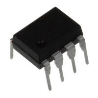
IC OPAMP LOW OFFSET 8-DIP

NJMOP-07D

Manufacturer Part Number
NJMOP-07D
Description
IC OPAMP LOW OFFSET 8-DIP
Manufacturer
NJR
Datasheet

Specifications of NJMOP-07D

Amplifier Type
General Purpose
Number Of Circuits
1
Slew Rate
0.17 V/µs
Gain Bandwidth Product
500kHz
Current - Input Bias
1.8nA
Voltage - Input Offset
60µV
Current - Supply
2.7mA
Voltage - Supply, Single/dual (±)
±3 V ~ 22 V
Operating Temperature
-40°C ~ 85°C
Mounting Type
Through Hole
Package / Case
8-DIP
Lead Free Status / RoHS Status
Contains lead / RoHS non-compliant
Output Type
-
Current - Output / Channel
-
-3db Bandwidth
-

Available stocks

Company
Part Number
Manufacturer
Quantity
Price
Part Number:
NJMOP-07D
Manufacturer:
JRC
Quantity:
5 510
Part Number:
NJMOP-07D
Manufacturer:
FUJ
Quantity:
5 510
■ GENERAL DESCRIPTION
current, low drift and high gain operational amplifier with internal
frequency compensation.
amplifier.
■ FEATURES
■ PIN CONFIGURATION
■ EQUIVALENT CIRCUIT
Ver.2003-03-18
● Low V
● Low I
● Low Drift
● Wide Operating Voltage
● Package Outline
● Bipolar Technology
The NJM OP-07 is ultra-low input offset voltage and bias
The NJM OP-07 is suitable for a precision instrumental
B
LOW OFFSET VOLTAGE,LOW DRIFT OPERATIONAL AMPLIFIER
IO
( 60µV )
( unnull 0.5µV/˚C )
( null 0.4µV/˚C )
( ±3V~±22V )
DIP8,DMP8
( 1.8nA )
( 0.4µV/M
o
)
NJMOP-07D
NJMOP-07M
PIN FUNCTION
1.
2.
3.
4.
5.
6.
7.
8.
■ PACKAGE OUTLINE
V
–INPUT
+INPUT
V
NC
OUTPUT
V
V
IO
-
+
IO
Trim
Trim
NJMOP-07D
NJMOP-07M
- 1 -

Related parts for NJMOP-07D

NJMOP-07D Summary of contents

Page 1

... Wide Operating Voltage ( ±3V~±22V ) ● Package Outline DIP8,DMP8 ● Bipolar Technology ■ PIN CONFIGURATION ■ EQUIVALENT CIRCUIT Ver.2003-03-18 ■ PACKAGE OUTLINE ) o PIN FUNCTION 1. V Trim IO 2. –INPUT 3. +INPUT - OUTPUT + Trim NJMOP-07D IO NJMOP-07M NJMOP-07D NJMOP-07M - 1 - ...

Page 2

ABSOLUTE MAXIMUM RATINGS PARAMETER Supply Voltage Input Voltage Differential Input Voltage Power Dissipation Storage Temperature Range Operating Temperature Range Output Current ( note1 ) For supply voltage less than ±22V. the absolute maximum input voltage is equal to the ...

Page 3

... Maximum Output Voltage ( note 1 ) Long Term Stability refers to the average trend line note 2 ) According to the evaluation by NJRC, more than 90 of all these products can be guaranteed. ■ OFFSET ADJUSTMENT METHOD For making low sensitivity of change in the input offset voltage against resistance regulation of potentiometer ‫ ...

Page 4

TYPICAL CHARACTERISTICS - 4 - Ver.2003-03-18 ...

Page 5

TYPICAL CHARACTERISTICS Ver.2003-03-18 [CAUTION] The specifications on this databook are only given for information , without any guarantee as regards either mistakes or omissions. The application circuits in this databook are described only to show representative usages of the ...

Related keywords