NJM4741M NJR, NJM4741M Datasheet
Home Integrated Circuits (ICs) Linear - Amplifiers - Instrumentation, OP Amps, Buffer Amps NJM4741M
Manufacturer Part Number
NJM4741M
Description
IC OPAMP QUAD GENERAL PURP 14DMP
Specifications of NJM4741M
Amplifier Type
General Purpose
Number Of Circuits
4
Slew Rate
1.6 V/µs
Gain Bandwidth Product
3.5MHz
Current - Input Bias
100nA
Voltage - Input Offset
1000µV
Current - Supply
7mA
Voltage - Supply, Single/dual (±)
±4 V ~ 20 V
Operating Temperature
-40°C ~ 85°C
Mounting Type
Surface Mount
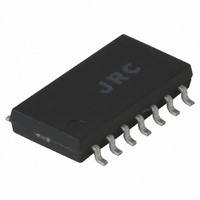
Package / Case
14-DMP
Number Of Channels
4
Voltage Gain Db
94 dB
Common Mode Rejection Ratio (min)
80 dB
Input Offset Voltage
5 mV
Supply Current
7 mA
Maximum Power Dissipation
300 mW
Maximum Operating Temperature
+ 85 C
Mounting Style
SMD/SMT
Maximum Dual Supply Voltage
+/- 20 V
Minimum Operating Temperature
- 40 C
Lead Free Status / RoHS Status
Contains lead / RoHS non-compliant
Output Type
-
Current - Output / Channel
-
-3db Bandwidth
-
Lead Free Status / Rohs Status
Details
Available stocks
Part Number:
NJM4741M -TE1
■ GENERAL DESCRIPTION
operational amplifiers that are designed for high slew rate, wide
band, and good noise characteristics.
■ FEATURES
■ PIN CONFIGURATION
■ EQUIVALENT CIRCUIT ( 1/4 Shown )
Ver.2003-03-18
● Operating Voltage
● Wide Band
● Slew Rate
● Low Input Noise Voltage
● Low Distortion
● Package Outline
● Bipolar Technology
The NJM4741 consists of four independent high-gain
GENERAL PURPOSE QUAD OPERATIONAL AMPLIFIER
( ±4V~±20V )
( 3.5MHz typ. )
( 1.6V/µs typ. )
( 9nV/Hzs typ. )
( 0.0005 typ. )
DIP14,DMP14
NJM4741D
NJM4741M
PIN FUNCTION
1.A OUTPUT
2.A –INPUT
3.A +INPUT
4.V
5.B +INPUT
6.B –INPUT
7.B OUTPUT
8.C OUTPUT
9.C –INPUT
10.C +INPUT
11. V
12.D +INPUT
13.D –INPUT
14.D OUTPUT
■ PACKAGE OUTLINE
+
-
NJM4741D
NJM4741M
- 1 -
Related parts for NJM4741M
NJM4741M Summary of contents
... DIP14,DMP14 PIN FUNCTION 1.A OUTPUT 2.A –INPUT 3.A +INPUT + 4.V 5.B +INPUT 6.B –INPUT 7.B OUTPUT 8.C OUTPUT 9.C –INPUT 10.C +INPUT - 11. V 12.D +INPUT NJM4741D 13.D –INPUT NJM4741M 14.D OUTPUT NJM4741M NJM4741D - 1 - ...
ABSOLUTE MAXIMUM RATINGS PARAMETER Supply Voltage Differential Input Voltage Input Voltage Power Dissipation Operating Temperature Range Storage Temperature Range ( note ) When the supply voltage is less than ±15V,the absolute maximum input voltage is equal to the supply ...
TYPICAL CHARACTERISTICS Ver.2003-03- ...
TYPICAL CHARACTERISTICS - 4 - Ver.2003-03-18 ...
TYPICAL CHARACTERISTICS Ver.2003-03-18 [CAUTION] The specifications on this databook are only given for information , without any guarantee as regards either mistakes or omissions. The application circuits in this databook are described only to show representative usages of the ...
Related keywords
njm4741 njm4741m njm4741d NJM4741M datasheet NJM4741M data sheet NJM4741M pdf datasheet NJM4741M component NJM4741M part NJM4741M distributor NJM4741M RoHS NJM4741M datasheet download