NJM13600M NJR, NJM13600M Datasheet
Home Integrated Circuits (ICs) Linear - Amplifiers - Instrumentation, OP Amps, Buffer Amps NJM13600M
Manufacturer Part Number
NJM13600M
Description
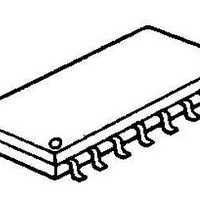
IC TRANSCONDUCT AMP DUAL 16-DMP
Specifications of NJM13600M
Amplifier Type
Transconductance
Number Of Circuits
2
Output Type
Push-Pull
Slew Rate
50 V/µs
Gain Bandwidth Product
2MHz
Current - Input Bias
400nA
Voltage - Input Offset
400µV
Current - Supply
2.6mA
Current - Output / Channel
650µA
Operating Temperature
-40°C ~ 85°C
Mounting Type
Surface Mount
Package / Case
16-DMP
Number Of Channels
2
Common Mode Rejection Ratio (min)
80 dB
Input Offset Voltage
5 mV
Supply Current
2.6 mA
Maximum Power Dissipation
700 mW
Maximum Operating Temperature
+ 85 C
Mounting Style
SMD/SMT
Maximum Dual Supply Voltage
+/- 18 V
Minimum Operating Temperature
- 40 C
Lead Free Status / RoHS Status
Contains lead / RoHS non-compliant
Voltage - Supply, Single/dual (±)
-
-3db Bandwidth
-
Lead Free Status / Rohs Status
Details
Available stocks
■ GENERAL DESCRIPTION
conductance amplifiers each with differential inputs and a push
pull output. The two amplifiers share common supplies but
otherwise operate independently. Linearizing diodes are
provided at the inputs to reduce distortion and allow higher input
levels. The result is a 10 dB signal-to-noise improvement
referenced to 0.5 percent THD.Controlled impedance buffers
are provided which are especially designed to complement the
dynamic range of the amplifiers.
■ FEATURES
■ PIN CONFIGURATION
■ EQUIVALENT CIRCUIT
Ver.2006-04-06
● Package Outline
● Bipolar Technology
The NJM13600/13700 consist of two current controlled trans
DUAL OPERATIONAL TRANSCONDUCTANCE AMPLIFIER
NJM13600D,NJM13600M
NJM13700D,NJM13700M
DIP16,DMP16
PIN FUNCTION
1.
2.
3.
4.
5.
6.
7.
8.
AMP BIAS INPUT A
DIODE BIAS A
+INPUT
–INPUT
OUTPUT A
V
BUFFER INPUT A
BUFFER OUTPUT A
■ PACKAGE OUTLINE
-
NJM13600D
NJM13700D
9. BUFFER OUTPUT B
10. BUFFER INPUT B
11. V
12. OUTPUT B
13. -INPUT B
14. +INPUT B
15. DIODE BIAS B
16. AMP BIAS INPUT B
+
NJM13600M
NJM13700M
- 1 -
Related parts for NJM13600M
NJM13600M Summary of contents
... PACKAGE OUTLINE NJM13600D NJM13700D PIN FUNCTION 1. AMP BIAS INPUT A 9. BUFFER OUTPUT B 2. DIODE BIAS A 10. BUFFER INPUT B 3. +INPUT 11 –INPUT 12. OUTPUT B 5. OUTPUT A 13. -INPUT 14. +INPUT B 7. BUFFER INPUT A 15. DIODE BIAS B 8. BUFFER OUTPUT A 16. AMP BIAS INPUT B NJM13600M NJM13700M + - 1 - ...
ABSOLUTE MAXIMUM RATINGS PARAMETER SYMBOL Supply Voltage V Differential Input Voltage Diode Bias Current Amp Bias Current Buffer Output Current Power Dissipation DC Input Voltage Operating Temperature Range Storage Temperature Range ( note ) ceramic PCB ...
TEST CIRCUIT Differential Input Current ■ TYPICAL APPLICATIONS Ver.2006-04-06 Leakage Current - 3 - ...
TYPICAL CHARACTERISTICS - 4 - Ver.2006-04-06 ...
TYPICAL CHARACTERISTICS Ver.2006-04- ...
TYPICAL CHARACTERISTICS - 6 - [CAUTION] The specifications on this databook are only given for information , without any guarantee as regards either mistakes or omissions. The application circuits in this databook are described only to show representative usages ...
Related keywords
njm13404 njm13700 njm13600 njm13700m njm13700d njm13600m njm13600d njm13404d njm13403v NJM13600M datasheet NJM13600M data sheet NJM13600M pdf datasheet NJM13600M component NJM13600M part NJM13600M distributor NJM13600M RoHS NJM13600M datasheet download