AD8568ART-R2 Analog Devices Inc, AD8568ART-R2 Datasheet
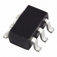
IC AMP BUF R-R DUAL 35MA SOT23-6

AD8568ART-R2

Manufacturer Part Number
AD8568ART-R2
Description
IC AMP BUF R-R DUAL 35MA SOT23-6
Manufacturer
Analog Devices Inc
Datasheet

Specifications of AD8568ART-R2

Rohs Status
RoHS non-compliant
Amplifier Type
Buffer
Number Of Circuits
2
Output Type
Rail-to-Rail
Slew Rate
6 V/µs
-3db Bandwidth
6MHz
Current - Input Bias
80nA
Voltage - Input Offset
2000µV
Current - Supply
700µA
Current - Output / Channel
35mA
Voltage - Supply, Single/dual (±)
4.5 V ~ 16 V
Operating Temperature
-40°C ~ 85°C
Mounting Type
Surface Mount
Package / Case
SOT-23-6
Gain Bandwidth Product
-
a
REV. C
Information furnished by Analog Devices is believed to be accurate and
reliable. However, no responsibility is assumed by Analog Devices for its
use, nor for any infringements of patents or other rights of third parties that
may result from its use. No license is granted by implication or otherwise
under any patent or patent rights of Analog Devices. Trademarks and
registered trademarks are the property of their respective owners.
GENERAL DESCRIPTION
The AD8568, AD8569, and AD8570 are low-cost, single-supply
buffer amplifiers with rail-to-rail input and output capability. They
are optimized for LCD monitor applications and built on an
advanced high voltage CBCMOS process. The AD8568 includes
two buffers, the AD8569 includes four buffers, and the AD8570
includes eight buffers.
These LCD buffers have high slew rates, 35 mA continuous
output drive, and high capacitive load drive capability. They
have a wide supply range and offset voltages below 10 mV.
The AD8568, AD8569, and AD8570 are specified over the –40°C
to +85°C temperature range. They are available on tape and reel,
with the AD8568 packaged in a 6-lead SOT-23, the AD8569
in a 10-lead MSOP, and the AD8570 in a 32-lead LFCSP and
20-lead TSSOP.
FEATURES
Single-Supply Operation: 4.5 V to 16 V
Input Capability Beyond the Rails
Rail-to-Rail Output Swing
Continuous Output Current: 35 mA
Peak Output Current: 250 mA
Offset Voltage: 10 mV Max
Slew Rate: 6 V/ s
Stable with 1 F Loads
Supply Current
APPLICATIONS
LCD Reference Drivers
Portable Electronics
Communications Equipment
One Technology Way, P.O. Box 9106, Norwood, MA 02062-9106, U.S.A.
Tel: 781/329-4700
Fax: 781/326-8703
AD8568/AD8569/AD8570
IN C 3
IN D 4
IN E 5
IN F 6
NC 2
NC 7
V+ 1
V+ 8
OUT B
IN 1
IN 2
IN 3
IN 4
IN 5
IN 6
IN 7
IN 8
OUT A
OUT A
PIN CONFIGURATIONS
V+
V+
GND
IN A
IN B
IN A
© 2003 Analog Devices, Inc. All rights reserved.
V+
10
1
2
3
4
5
6
7
8
9
NC = NO CONNECT
32-Lead LFCSP
20-Lead TSSOP
6-Lead SOT-23
10-Lead MSOP
3
4
5
1
2
1
2
3
AD8570-ARU
(RM Suffix)
(RT Suffix)
(CP Suffix)
PIN 1
INDICATOR
AD8570
TOP VIEW
TOP VIEW
AD8569
AD8568
Buffer Amplifiers
16 V Rail-to-Rail
10
6
5
4
9
8
7
6
20
19
18
17
16
15
14
13
12
11
OUT D
IN D
IN C
OUT C
OUT B
V+
IN B
GND
24 GND
23 NC
22 OUT C
21 OUT D
20 OUT E
19 OUT F
18 NC
17 GND
OUT 1
OUT 2
V–
OUT 3
OUT 4
OUT 5
OUT 6
V–
OUT 7
OUT 8
www.analog.com

Related parts for AD8568ART-R2

AD8568ART-R2 Summary of contents

Page 1

FEATURES Single-Supply Operation: 4 Input Capability Beyond the Rails Rail-to-Rail Output Swing Continuous Output Current Peak Output Current: 250 mA Offset Voltage Max Slew Rate Stable with 1 ...

Page 2

AD8568/AD8569/AD8570–SPECIFICATIONS ELECTRICAL CHARACTERISTICS Parameter INPUT CHARACTERISTICS Offset Voltage Offset Voltage Drift Input Bias Current Input Voltage Range Input Impedance Input Capacitance OUTPUT CHARACTERISTICS Output Voltage High Output Voltage Low Continuous Output Current Peak Output Current TRANSFER CHARACTERISTICS Gain Gain Linearity ...

Page 3

... This is a stress rating only; functional operation of the device at these or any other conditions above those listed in the operational sections of this specification is not implied. Exposure to absolute maximum rating conditions for extended periods may affect device reliability. Model AD8568ART-R2 AD8568ART-REEL AD8568ART-REEL7 AD8569ARM-R2 AD8569ARM-REEL ...

Page 4

AD8568/AD8569/AD8570 100 4.5V < V < 16V INPUT OFFSET VOLTAGE (mV) TPC 1. Input Offset Voltage Distribution 300 250 ...

Page 5

I = 5mA LOAD 135 120 105 4. TEMPERATURE ( C) TPC 7. Output Voltage Swing vs. Temperature 0.9999 R L 0.9997 R L 0.9995 ...

Page 6

AD8568/AD8569/AD8570 560 50mV rms 40pF 100k 1M FREQUENCY (Hz) TPC ...

Page 7

4.5V V 16V S 100 100 FREQUENCY (Hz) TPC 19. Voltage Noise Density vs. Frequency 4.5V < V < 16V ...

Page 8

AD8568/AD8569/AD8570 TIME (2 s/DIV) TPC 25. Large Signal Transient Response TIME (1 ...

Page 9

APPLICATIONS Theory of Operation This family of buffers is designed to drive large capacitive loads in LCD applications. Each has high output current drive and rail- to-rail input/output operation and can be powered from a single 16 V supply. They ...

Page 10

AD8568/AD8569/AD8570 6-Lead Small Outline Transistor Package [SOT-23] (RT-6) Dimensions shown in millimeters 2.90 BSC 2.80 BSC 1.60 BSC PIN 1 0.95 BSC 1.90 1.30 BSC 1.15 0.90 1.45 MAX 0.50 0.15 MAX SEATING 0.30 ...

Page 11

Thin Shrink Small Outline Package [TSSOP] 0.15 0.05 COPLANARITY 0.10 Revision History Location 12/03—Data Sheet changed from REV REV. C. Updated ORDERING GUIDE . . . . . . . . . . . . . . ...

Page 12

–12– ...

Related keywords