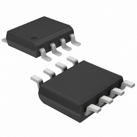
ICL7621DCSA Maxim Integrated Products, ICL7621DCSA Datasheet - Page 12

ICL7621DCSA
Manufacturer Part Number
ICL7621DCSA
Description
IC OPAMP DUAL LP CMOS 8-SOIC
Manufacturer
Maxim Integrated Products
Datasheet
1.ICL7621DCSA.pdf
(26 pages)
Specifications of ICL7621DCSA
Amplifier Type
General Purpose
Number Of Circuits
2
Output Type
Rail-to-Rail
Slew Rate
0.16 V/µs
Gain Bandwidth Product
480kHz
Current - Input Bias
1pA
Voltage - Input Offset
15000µV
Current - Supply
100µA
Voltage - Supply, Single/dual (±)
2 V ~ 16 V, ±1 V ~ 8 V
Operating Temperature
0°C ~ 70°C
Mounting Type
Surface Mount
Package / Case
8-SOIC (3.9mm Width)
Lead Free Status / RoHS Status
Contains lead / RoHS non-compliant
Current - Output / Channel
-
-3db Bandwidth
-
Available stocks
Company
Part Number
Manufacturer
Quantity
Price
Company:
Part Number:
ICL7621DCSA
Manufacturer:
MAXIM
Quantity:
187
Part Number:
ICL7621DCSA
Manufacturer:
INTERSIL
Quantity:
20 000
Company:
Part Number:
ICL7621DCSA+T
Manufacturer:
SONY
Quantity:
6 218
Total Supply Voltage (V+ to V-) ...........................................+18V
Input Voltage ........................................(V+ + 0.3V) to (V- - 0.3V)
Differential Input Voltage (Note 5).......±|(V+ + 0.3V) - (V- - 0.3V)
Duration of Output Short Circuit (Note 6) ......................Unlimited
Continuous Power Dissipation (T
Single/Dual/Triple/Quad
Operational Amplifiers
ABSOLUTE MAXIMUM RATINGS (Triple/Quad)
ELECTRICAL CHARACTERISTICS (Triple/Quad)
(V
Stresses beyond those listed under “Absolute Maximum Ratings” may cause permanent damage to the device. These are stress ratings only, and functional
operation of the device at these or any other conditions beyond those indicated in the operational sections of the specifications is not implied. Exposure to
absolute maximum rating conditions for extended periods may affect device reliability.
Note 5: Long-term offset voltage stability will be degraded if large input differential voltages are applied for long periods of time.
Note 6: The outputs may be shorted to ground or to either supply for V SUPP ≤ 10V. Care must be taken to insure that the
12
Input Offset Voltage
Temperature
Coefficient of V
Input Offset Current
Input Bias Current
Common-Mode
Voltage Range
Output Voltage
Swing
Large-Signal Voltage
Gain
Unity-Gain
Bandwidth
Input Resistance
Common-Mode
Rejection Ratio
SUPP
TO-99 Metal Can (derate 2mW/°C above +25°C) .......250mW
8-Pin Minidip (derate 2mW/°C above +25°C) ..............250mW
14-Pin Plastic (derate 3mW/°C above +25°C) .............375mW
14-Pin CERDIP (derate 4mW/°C above +25°C)...........500mW
PARAMETER
______________________________________________________________________________________
= ±1.0V, I
dissipation rating is not exceeded.
OS
Q
= 10µA, T
SYMBOL
∆V
CMRR
V
V
A
GBW
I
V
BIAS
I
R
OS
CMR
OUT
OS
VOL
OS
IN
A
/∆T
= +25°C, unless otherwise noted.) (Specifications apply to ICL7631/7632/7642 only.)
A
= +25°C)
R
T
R
T
R
T
0°C ≤ T
T
0°C ≤ T
R
R
+70°C
V
T
V
0°C ≤ T
R
A
MIN
A
A
A
S
S
S
L
L
O
O
S
≤ 100kΩ,
= +25°C
≤ 100kΩ,
≤ 100kΩ
= +25°C
= +25°C
= 1MΩ, T
= 1MΩ, 0°C ≤ T
= +25°C
≤ 100kΩ
= ±0.1V, R
= ±0.1V, R
CONDITIONS
≤ T
A
A
A
A
≤ +70°C
≤ +70°C
≤ +70°C
≤ T
A
MAX
L
L
= +25°C
= 1MΩ,
= 1MΩ,
A
≤
MIN
-0.4
Operating Temperature Ranges:
M Series .............................................................-55°C to +125°C
E Series................................................................-40°C to +85°C
C Series .................................................................-0°C to +70°C
Storage Temperature Range ............................-55°C to +150°C
Lead Temperature (soldering, 10s) ................................+300°C
16-Pin Plastic (derate 3mW/°C above +25°C) .............375mW
16-Pin CERDIP (derate 4mW/°C above +25°C)...........500mW
ICL76XXB
±0.98
±0.96
0.044
TYP
10
0.5
1.0
15
90
80
80
12
MAX
+0.6
300
500
30
50
5
7
MIN
-0.4
ICL76XXC
±0.98
±0.96
0.044
TYP
10
0.5
1.0
20
90
80
80
12
MAX
+0.6
300
500
10
12
30
50
UNITS
µV/°C
MHz
mV
pA
pA
dB
dB
Ω
V
V


