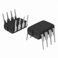
MC34071PG ON Semiconductor, MC34071PG Datasheet - Page 2

MC34071PG
Manufacturer Part Number
MC34071PG
Description
IC OPAMP SGL SUPPLY 4.5MHZ 8DIP
Manufacturer
ON Semiconductor
Specifications of MC34071PG
Amplifier Type
General Purpose
Number Of Circuits
1
Slew Rate
13 V/µs
Gain Bandwidth Product
4.5MHz
Current - Input Bias
100nA
Voltage - Input Offset
1000µV
Current - Supply
1.9mA
Current - Output / Channel
30mA
Voltage - Supply, Single/dual (±)
3 V ~ 44 V, ±1.5 V ~ 22 V
Operating Temperature
0°C ~ 70°C
Mounting Type
Through Hole
Package / Case
8-DIP (0.300", 7.62mm)
Bandwidth
4.5 MHz
Channel Separation
120
Common Mode Rejection Ratio
97
Current, Input Bias
700 nA
Current, Input Offset
300 nA
Current, Output
30 mA
Current, Supply
2.8 mA
Harmonic Distortion
0.02 %
Number Of Amplifiers
Single
Package Type
PDIP-8
Resistance, Input
150 Megohms
Temperature, Operating, Range
0 to +70 °C
Voltage, Gain
20 V/mV
Voltage, Input
±15 V
Voltage, Noise
32 nV/sqrt Hz
Voltage, Offset
7 mV
Voltage, Output, High
13.4 V
Voltage, Output, Low
-13.5 V
Voltage, Supply
3 to 44 V
Number Of Channels
1
Voltage Gain Db
100 dB
Common Mode Rejection Ratio (min)
70 dB
Input Voltage Range (max)
Positive Rail - 1.8 V
Input Voltage Range (min)
Negative Rail
Input Offset Voltage
5 mV
Operating Supply Voltage
44 V
Supply Current
1.9 mA
Maximum Operating Temperature
+ 70 C
Mounting Style
Through Hole
Maximum Dual Supply Voltage
+/- 22 V
Minimum Operating Temperature
0 C
Lead Free Status / RoHS Status
Lead free / RoHS Compliant
Output Type
-
-3db Bandwidth
-
Lead Free Status / Rohs Status
RoHS Compliant part
Electrostatic Device
Other names
MC34071PGOS
Stresses exceeding Maximum Ratings may damage the device. Maximum Ratings are stress ratings only. Functional operation above the
Recommended Operating Conditions is not implied. Extended exposure to stresses above the Recommended Operating Conditions may affect
device reliability.
1. Either or both input voltages should not exceed the magnitude of V
2. Power dissipation must be considered to ensure maximum junction temperature (T
MAXIMUM RATINGS
Supply Voltage (from V
Input Differential Voltage Range
Input Voltage Range
Output Short Circuit Duration (Note 2)
Operating Junction Temperature
Storage Temperature Range
Offset Null
Inputs
Inputs 1
Output 1
Inputs
CASE 626/CASE 751
V
V
EE
EE
-
+
1
2
3
4
(Single, Top View)
(Dual, Top View)
2
3
4
1
+
-
-
+
Q1
Bias
EE
-
+
Q2
8
7
6
5
to V
8
7
6
5
Output 2
V
NC
V
Output
Offset Null
CC
CC
Inputs 2
CC
Rating
Q3
Q8
)
Cancellation
Current
Base
(MC33071, MC34071 only)
Figure 1. Representative Schematic Diagram
Offset Null
R1
Inputs 1
Inputs 2
Output 1
Q4
Output 2
Q9
CASE 646/CASE 751A/CASE 948G
V
R3
Q12
D1
CC
C1
1
2
3
4
5
6
7
PIN CONNECTIONS
Q10
http://onsemi.com
(Quad, Top View)
+
-
-
+
Q13
(Each Amplifier)
R2
R4
2
1
3
4
2
CC
Q5
-
+
+
-
or V
14
13
12
11
10
9
8
Q11
Output 4
V
Output 3
EE
EE
Q14
Symbol
Inputs 4
Inputs 3
.
V
T
V
t
V
T
SC
IDR
stg
IR
S
J
Q6
J
) is not exceeded (see Figure 2).
C2
Q15
Output 1
Q7
R5
In + 1
In 1
D2
NC
Q16
Q17
−60 to +150
Indefinite
D3
(Note 1)
(Note 1)
2
3
4
R6
Value
1
+150
+44
CASE 510AJ
R7
(Top View)
VEE/GND
Current
VCC
10
Q18
Q19
5
Limit
R8
V
EE
V
/GND
CC
Output
9
8
7
6
Unit
Sec
°C
°C
V
V
V
Output 2
NC
In 2
In + 2


