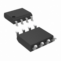
LMH6619MA/NOPB National Semiconductor, LMH6619MA/NOPB Datasheet - Page 7

LMH6619MA/NOPB
Manufacturer Part Number
LMH6619MA/NOPB
Description
IC AMP DUAL RRIO 130MHZ 8-SOIC
Manufacturer
National Semiconductor
Series
PowerWise®r
Specifications of LMH6619MA/NOPB
Amplifier Type
Voltage Feedback
Number Of Circuits
2
Output Type
Rail-to-Rail
Slew Rate
57 V/µs
Gain Bandwidth Product
58MHz
-3db Bandwidth
140MHz
Current - Input Bias
1.5µA
Voltage - Input Offset
100µV
Current - Supply
1.45mA
Current - Output / Channel
35mA
Voltage - Supply, Single/dual (±)
2.7 V ~ 11 V, ±1.35 V ~ 5.5 V
Operating Temperature
-40°C ~ 125°C
Mounting Type
Surface Mount
Package / Case
8-SOIC (3.9mm Width)
Bandwidth
130 MHz
Common Mode Rejection Ratio
96
Current, Input Bias
1 μA (NPN Active), -1.5 μA (PNP Active)
Current, Input Offset
0.01 μA
Current, Output
±35 mA
Current, Supply
1.3 mA
Impedance, Thermal
160 °C/W
Number Of Amplifiers
Dual
Package Type
SOIC-8
Resistance, Input
8 Megohms
Temperature, Operating, Range
-40 to +125 °C
Time, Fall
30 ns
Time, Rise
30 ns
Voltage, Gain
100 dB
Voltage, Input
2.7 to 11 V
Voltage, Noise
10 nV/sqrt Hz
Voltage, Offset
0.1 mV
Voltage, Output, High
230 mV
Voltage, Output, Low
255 mV
Voltage, Supply
5 V
Number Of Channels
2
Voltage Gain Db
100 dB
Common Mode Rejection Ratio (min)
81 dB
Input Offset Voltage
0.6 mV at 5 V
Operating Supply Voltage
3 V, 5 V, 9 V
Supply Current
3 mA at 5 V
Maximum Operating Temperature
+ 125 C
Minimum Operating Temperature
- 40 C
For Use With
551600075-001 - BOARD FOR SOIC LMH6612/19551600074-001 - BOARD FOR SOIC LMH6612/19
Lead Free Status / RoHS Status
Lead free / RoHS Compliant
Other names
LMH6619MA
Output DC Characteristics
V
I
R
Enable Pin Operation
t
t
Power Supply Performance
PSRR
I
I
Symbol
OUT
on
off
S
SD
OUT
OUT
Note 1: Absolute Maximum Ratings indicate limits beyond which damage to the device may occur. Operating Ratings indicate conditions for which the device is
intended to be functional, but specific performance is not guaranteed. For guaranteed specifications and the test conditions, see the Electrical Characteristics.
Note 2: Human Body Model, applicable std. MIL-STD-883, Method 3015.7. Machine Model, applicable std. JESD22-A115-A (ESD MM std. of JEDEC)
Field-Induced Charge-Device Model, applicable std. JESD22-C101-C (ESD FICDM std. of JEDEC).
Note 3: The maximum power dissipation is a function of T
P
Note 4: Boldface limits apply to temperature range of −40°C to 125°C
Note 5: Voltage average drift is determined by dividing the change in V
Note 6: Do not short circuit the output. Continuous source or sink currents larger than the I
Note 7: Typical values represent the most likely parametric norm as determined at the time of characterization. Actual typical values may vary over time and will
also depend on the application and configuration. The typical values are not tested and are not guaranteed on shipped production material.
Note 8: Limits are 100% production tested at 25°C. Limits over the operating temperature range are guaranteed through correlations using the Statistical Quality
Control (SQC) method.
D
= (T
J(MAX
Output Voltage Swing High (LMH6618)
(Voltage from V
Output Voltage Swing Low (LMH6618)
(Voltage from V
Output Voltage Swing High (LMH6619)
(Voltage from V
Output Voltage Swing Low (LMH6619)
(Voltage from V
Linear Output Current
Output Resistance
Enable High Voltage Threshold
Enable Pin High Current
Enable Low Voltage Threshold
Enable Pin Low Current
Turn-On Time
Turn-Off Time
Power Supply Rejection Ratio
Supply Current (LMH6618)
Supply Current (LMH6619)
(per channel)
Disable Shutdown Current
) – T
A
)/ θ
JA
. All numbers apply for packages soldered directly onto a PC Board.
Parameter
+
−
+
−
Supply Rail)
Supply Rail)
Supply Rail)
Supply Rail)
J(MAX)
R
R
R
R
R
R
R
R
R
R
V
f = 1 MHz
Enabled
V
Disabled
V
DC, V
R
R
DISABLE = −5V
OUT
DISABLE
DISABLE
L
L
L
L
L
L
L
L
L
L
L
L
, θ
= 1 kΩ to GND
= 150Ω to GND
= 1 kΩ to GND
= 150Ω to GND
= 150Ω to V
= 1 kΩ to GND
= 150Ω to GND
= 1 kΩ to GND
= 150Ω to GND
= 150Ω to V
=
=
JA
∞
∞
= V
CM
. The maximum allowable power dissipation at any ambient temperature is
OS
+
= +5V
= −5V
= −4.5V, V
/2 (Note 6)
by temperature change.
Condition
7
−
−
S
= 2.7V to 11V
OUT
typical are not recommended as it may damage the part.
(Note 8)
Min
±25
0.5
84
(Note 7)
0.17
1.35
1.45
Typ
100
430
110
440
100
430
115
450
±35
104
103
35
45
16
17
25
90
(Note 8)
Max
−0.5
1.65
111
126
457
526
121
136
474
559
111
126
457
526
126
141
484
569
140
1.6
1.9
2.0
51
52
61
62
either rail
either rail
mV from
mV from
Units
mA
mA
µA
µA
dB
μA
ns
ns
Ω
V
V


