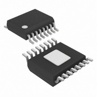
ISL28274FAZ Intersil, ISL28274FAZ Datasheet - Page 16

ISL28274FAZ
Manufacturer Part Number
ISL28274FAZ
Description
IC INSTR/OP AMP RRIO SGL 16-QSOP
Manufacturer
Intersil
Datasheet
1.ISL28474EVAL1Z.pdf
(18 pages)
Specifications of ISL28274FAZ
Amplifier Type
Instrumentation
Number Of Circuits
2
Output Type
Rail-to-Rail
Slew Rate
0.5 V/µs
Gain Bandwidth Product
6MHz
Current - Input Bias
10pA
Voltage - Input Offset
35µV
Current - Supply
120µA
Current - Output / Channel
31mA
Voltage - Supply, Single/dual (±)
2.4 V ~ 5 V, ±1.2 V ~ 2.5 V
Operating Temperature
-40°C ~ 125°C
Mounting Type
Surface Mount
Package / Case
16-QSOP
Lead Free Status / RoHS Status
Lead free / RoHS Compliant
-3db Bandwidth
-
Available stocks
Company
Part Number
Manufacturer
Quantity
Price
Company:
Part Number:
ISL28274FAZ
Manufacturer:
Intersil
Quantity:
250
Input Stage and Input Voltage Range
The input terminals (IN+ and IN-) of both amplifiers “A” and
“B” are single differential pair P-MOSFET devices aided by
an Input Range Enhancement Circuit to increase the
headroom of operation of the common-mode input voltage.
The feedback terminals (FB+ and FB-) of amplifier “A” also
have a similar topology. As a result, the input common-mode
voltage range is rail-to-rail. These amps are able to handle
input voltages that are at or slightly beyond the supply and
ground making them well suited for single 5V or 3.3V low
voltage supply systems. There is no need then to move the
common-mode input to achieve symmetrical input voltage.
Output Stage and Output Voltage Range
A pair of complementary MOSFET devices drives the output
V
the PMOS sources current and pulls the output up to 4mV
below the positive supply, while the NMOS sinks current and
pulls the output down to 3mV above the negative supply, or
ground in the case of a single supply operation. The current
sinking and sourcing capability of the ISL28274 are internally
limited to 31mA.
Gain Setting of Instrumentation Amp “A”
VIN, the potential difference across IN+ and IN-, is replicated
(less the input offset voltage) across FB+ and FB-. The goal
of the ISL28274 in-amp is to maintain the differential voltage
across FB+ and FB- equal to IN+ and IN-;
(FB+ - FB-) = (IN+ - IN-). Consequently, the transfer function
can be derived. The gain is set by two external resistors, the
feedback resistor R
In Figure 61, the FB+ pin and one end of resistor R
connected to GND. With this configuration, Equation 1 is
only true for a positive swing in VIN; negative input swings
will be ignored and the output will be at ground.
VOUT
OUT
FIGURE 61. GAIN IS BY EXTERNAL RESISTORS R
VCM
to within a few mV of the supply rails. At a 100kΩ load,
=
⎛
⎜
⎝
1
VIN/2
VIN/2
+
------- -
R
R
G
F
⎞
⎟
⎠
VIN
RG
F,
and the gain resistor R
6
5
3
4
FB+
FB-
16
IN+
IN-
2.4V TO 5V
+
+
-
-
16
ISL28274
8
RF
V
V
+
-
7
G
2
.
AMP “A”
F
ISL28274, ISL28474
G
AND R
VOUT
are
(EQ. 1)
G
Reference Connection
Unlike a three-op amp instrumentation amplifier, a finite
series resistance seen at the REF terminal does not degrade
the high CMRR performance, eliminating the need for an
additional external buffer amplifier. Figure 62 uses the FB+
pin to provide a high impedance REF terminal.
The FB+ pin is used as a REF terminal to center or to adjust
the output. Because the FB+ pin is a high impedance input,
an economical resistor divider can be used to set the voltage
at the REF terminal without degrading or affecting the CMRR
performance. Any voltage applied to the REF terminal will
shift V
by resistors R
The FB+ pin can also be connected to the other end of resistor,
R
maintain constant differential voltage across the input terminals
and feedback terminals (IN+ - IN- = FB+ - FB-), the transfer
function of Figure 63 can be derived.
VOUT
FIGURE 62. GAIN SETTING AND REFERENCE CONNECTION
G
FIGURE 63. REFERENCE CONNECTION WITH AN AVAILABLE
. See Figure 63. Keeping the basic concept that the in-amps
VCM
VCM
VREF
REF
2.4V to 5V
OUT
=
⎛
⎜
⎝
1
R1
R2
VIN/2
VIN/2
VIN/2
VIN/2
by V
+
VREF
------- -
R
R
F
G
F
REF
and R
⎞
⎟
⎠
(
VIN
RG
RG
times the closed loop gain, which is set
G
)
+
as shown in Figure 62.
⎛
⎜
⎝
1
6
5
3
4
6
5
3
4
+
FB+
FB-
FB+
FB-
IN+
IN-
IN+
IN-
------- -
R
R
G
F
2.4V TO 5V
2.4V TO 5V
⎞
⎟
⎠
+
+
+
+
-
-
-
-
(
16
16
ISL28274
ISL28274
8
VREF
8
RF
RF
V
V
V
V
+
+
-
-
7
7
)
2
2
AMP “A”
AMP “A”
May 14, 2009
VOUT
VOUT
FN6345.3
(EQ. 2)


