ISL28271FAZ Intersil, ISL28271FAZ Datasheet - Page 11
ISL28271FAZ
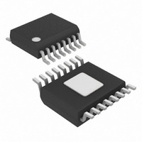
Manufacturer Part Number
ISL28271FAZ
Description
IC INSTR AMP RRIO SGL 16-QSOP
Manufacturer
Intersil
Datasheet
1.ISL28271INEVAL1Z.pdf
(14 pages)
Specifications of ISL28271FAZ
Amplifier Type
Instrumentation
Number Of Circuits
2
Output Type
Rail-to-Rail
Slew Rate
0.5 V/µs
-3db Bandwidth
180kHz
Current - Input Bias
10pA
Voltage - Input Offset
35µV
Current - Supply
120µA
Current - Output / Channel
31mA
Voltage - Supply, Single/dual (±)
2.4 V ~ 5.5 V, ±1.2 V ~ 2.75 V
Operating Temperature
-40°C ~ 125°C
Mounting Type
Surface Mount
Package / Case
16-QSOP
Lead Free Status / RoHS Status
Lead free / RoHS Compliant
Gain Bandwidth Product
-


Application Information
Product Description
The ISL28271 and ISL28272 are dual channel micropower
instrumentation amplifiers (in-amps) which deliver rail-to-rail
input amplification and rail-to-rail output swing. The in-amps
also deliver excellent DC and AC specifications while
consuming only about 120µA for both channels. Because
the independent pair of feedback terminals set the gain and
adjust the output zero level, the ISL28271 and ISL28272
achieve high CMRR regardless of the tolerance of the gain
setting resistors. The ISL28271 is internally compensated for
a minimum gain of 10. The ISL28272 is internally
compensated for a minimum gain of 100.
EN pins are available to independently enable or disable a
channel. When all channels are off, current consumption is
down to typically 4µA.
Input Protection
All input terminals and feedback terminals have internal ESD
protection diodes to both positive and negative supply rails,
limiting the input voltage to within one diode beyond the
supply rails. Input signals originating from low impedance
sources should have current limiting resistors in series with
the IN+ and IN- pins to prevent damaging currents during
power supply sequencing and other transient conditions.
The ISL28272 has additional back-to-back diodes across the
input terminals and also across the feedback terminals. If
overdriving the inputs is necessary, the external input current
must never exceed 5mA. External series resistors may be
used as an external protection to limit excessive external
voltage and current from damaging the inputs. On the other
hand, the ISL28271 has no clamps to limit the differential
voltage on the input terminals allowing higher differential
input voltages at lower gain applications. It is recommended
however, that the terminals of the ISL28271 are not
overdriven beyond 1V to avoid offset drift.
Input Stage and Input Voltage Range
The input terminals (IN+ and IN-) of the in-amps are a single
differential pair of CMOS devices aided by an Input Range
Enhancement Circuit, IREC, to increase the headroom of
operation of the common-mode input voltage. The feedback
terminals (FB+ and FB-) also have a similar topology. As a
result, the input common-mode voltage range is rail-to-rail
regardless of the feedback terminal settings and regardless
of the gain settings. They are able to handle input voltages
that are at or slightly beyond the supply and ground sensing
making these in-amps well suited for single 5V down to 2.4V
supply systems.
The IREC enables rail-to-rail input amplification without the
problems usually associated with the dual differential stage
topology. The IREC ensures that there are no drastic
changes in offset voltage over the entire range of the input.
See Input Offset Voltage vs Common-Mode Input Voltage in
11
ISL28271, ISL28272
performance charts. IREC also cures the abrupt change and
even reverse polarity of the input bias current over the whole
range of input.
Output Stage and Output Voltage Range
A Class AB common-source output stage drives the output.
The pair of complementary MOSFET devices drive the
output VOUT to within a few millivolts of the supply rails. At a
100kΩ load, the PMOS sources current and pulls the output
up to 4mV below the positive supply. The NMOS sinks
current and pulls the output down to 4mV above the negative
supply, or ground in the case of a single supply operation.
The current sinking and sourcing capability are internally
limited to 31mA. When disabled, the outputs are in a high
impedance state.
Gain Setting
VIN, the potential difference across IN+ and IN-, is replicated
(less the input offset voltage) across FB+ and FB-. The
function of the in-amp is to maintain the differential voltage
across FB- and FB+ equal to IN+ and IN-; (FB- - FB+) =
(IN+ - IN-). Consequently, the transfer function can be
derived. The in-amp gain is set by two external resistors, the
feedback resistor R
In Figure 37, the FB+ pin and one end of resistor RG are
connected to GND. With this configuration, Equation 1 is
only true for a positive swing in VIN; negative input swings
will be ignored because the output will be at ground.
Reference Connection
Unlike a three op amp in-amp realization, a finite series
resistance seen at the REF terminal does not degrade the
high CMRR performance eliminating the need for an
additional external buffer amplifier. Figure 38 uses the FB+
pin to provide a high impedance REF terminal.
VIN
VOUT
FIGURE 37. GAIN IS SET BY TWO EXTERNAL RESISTORS,
VCM
=
IN+ IN-
=
IN+
IN-
⎛
⎜
⎝
1
–
+
R
------- -
R
R
F
G
F
RG
AND R
⎞
⎟
⎠
VIN
F
, and the gain resistor R
G
FB+
FB-
IN+
IN-
2.4V TO 5.5V
+
+
-
-
RF
V+
ISL28271
ISL28272
V-
EN
G
.
August 17, 2007
EN
FN6390.2
(EQ. 1)
VOUT
Related parts for ISL28271FAZ
Image
Part Number
Description
Manufacturer
Datasheet
Request
R

Part Number:
Description:
Intersil Corporation [CMOS Serial Controller Interface]
Manufacturer:
Intersil Corporation
Datasheet:
Part Number:
Description:
Manufacturer:
Intersil Corporation
Datasheet:
Part Number:
Description:
357-036-542-201 CARDEDGE 36POS DL .156 BLK LOPRO
Manufacturer:
Intersil Corporation
Datasheet:
Part Number:
Description:
1024-Word x 4-Bit LSI Static RAM
Manufacturer:
Intersil Corporation
Datasheet:
Part Number:
Description:
General Purpose NPN Transistor Arrays FN341.4
Manufacturer:
Intersil Corporation
Datasheet:
Part Number:
Description:
CMOS 16-Bit Microprocessor
Manufacturer:
Intersil Corporation
Datasheet:
Part Number:
Description:
Manufacturer:
Intersil Corporation
Datasheet:
Part Number:
Description:
Manufacturer:
Intersil Corporation
Datasheet:
Part Number:
Description:
Manufacturer:
Intersil Corporation
Datasheet:
Part Number:
Description:
Manufacturer:
Intersil Corporation
Datasheet:
Part Number:
Description:
CMOS 6-Bit Latch and Decoder Memory Interfaces
Manufacturer:
Intersil Corporation
Datasheet:
Part Number:
Description:
CA3046General Purpose NPN Transistor Arrays
Manufacturer:
Intersil Corporation
Datasheet:
Part Number:
Description:
Manufacturer:
Intersil Corporation
Datasheet:
Part Number:
Description:
TR909 DLC/FLC SLIC with Low Power Standby
Manufacturer:
Intersil Corporation
Datasheet:
Part Number:
Description:
Manufacturer:
Intersil Corporation
Datasheet: