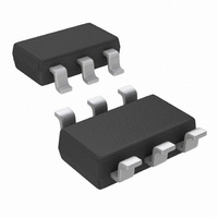
LMP7711MKE/NOPB National Semiconductor, LMP7711MKE/NOPB Datasheet - Page 14

LMP7711MKE/NOPB
Manufacturer Part Number
LMP7711MKE/NOPB
Description
IC OP AMP PREC 14MHZ LN TSOT23-6
Manufacturer
National Semiconductor
Series
LMP®, PowerWise®r
Datasheet
1.LMP7712MMNOPB.pdf
(20 pages)
Specifications of LMP7711MKE/NOPB
Amplifier Type
General Purpose
Number Of Circuits
1
Output Type
Rail-to-Rail
Slew Rate
11.5 V/µs
Gain Bandwidth Product
17MHz
Current - Input Bias
0.1pA
Voltage - Input Offset
10µV
Current - Supply
1.15mA
Current - Output / Channel
66mA
Voltage - Supply, Single/dual (±)
1.8 V ~ 5.5 V
Operating Temperature
-40°C ~ 125°C
Mounting Type
Surface Mount
Package / Case
TSOT-23-6, TSOT-6
Lead Free Status / RoHS Status
Lead free / RoHS Compliant
-3db Bandwidth
-
Other names
LMP7711MKE
www.national.com
Application Notes
LMP7711/LMP7712
The LMP7711/LMP7712 are single and dual, low noise, low
offset, rail-to-rail output precision amplifiers with a wide gain
bandwidth product of 17 MHz and low supply current. The
wide bandwidth makes the LMP7711/LMP7712 ideal choices
for wide-band amplification in portable applications. The low
supply current along with the enable feature that is built-in on
the LMP7711/LMP7712 allows for even more power efficient
designs by turning the device off when not in use.
The LMP7711/LMP7712 are superior for sensor applications.
The very low input referred voltage noise of only 5.8 nV/
at 1 kHz and very low input referred current noise of only 10
fA/
ratio.
The LMP7711/LMP7712 have a supply voltage range of 1.8V
to 5.5V over a wide temperature range of 0°C to 125°C. This
is optimal for low voltage commercial applications. For appli-
cations where the ambient temperature might be less than 0°
C, the LMP7711/LMP7712 are fully operational at supply volt-
ages of 2.0V to 5.5V over the temperature range of −40°C to
125°C.
The outputs of the LMP7711/LMP7712 swing within 25 mV of
either rail providing maximum dynamic range in applications
requiring low supply voltage. The input common mode range
of the LMP7711/LMP7712 extends to 300 mV below ground.
This feature enables users to utilize this device in single sup-
ply applications.
The use of a very innovative feedback topology has enhanced
the current drive capability of the LMP7711/LMP7712, result-
ing in sourcing currents as much as 47 mA with a supply
voltage of only 1.8V.
The LMP7711 is offered in the space saving TSOT23 pack-
age and the LMP7712 is offered in a 10-pin MSOP. These
small packages are ideal solutions for applications requiring
minimum PC board footprint.
National Semiconductor is heavily committed to precision
amplifiers and the market segments they serves. Technical
support and extensive characterization data is available for
sensitive applications or applications with a constrained error
budget.
Closed Loop Output Impedance vs. Frequency
mean more signal fidelity and higher signal-to-noise
20150332
14
CAPACITIVE LOAD
The unity gain follower is the most sensitive configuration to
capacitive loading. The combination of a capacitive load
placed directly on the output of an amplifier along with the
output impedance of the amplifier creates a phase lag which
in turn reduces the phase margin of the amplifier. If phase
margin is significantly reduced, the response will be either
underdamped or the amplifier will oscillate.
The LMP7711/LMP7712 can directly drive capacitive loads of
up to 120 pF without oscillating. To drive heavier capacitive
loads, an isolation resistor, R
This resistor and C
lag or increase the phase margin of the overall system. The
larger the value of R
will be. However, larger values of R
swing and reduced output current drive.
INPUT CAPACITANCE
CMOS input stages inherently have low input bias current and
higher input referred voltage noise. The LMP7711/LMP7712
enhance this performance by having the low input bias current
of only 50 fA, as well as, a very low input referred voltage
noise of 5.8 nV/
stage has been used. This larger input stage increases the
input capacitance of the LMP7711/LMP7712. Figure 2 shows
typical input common mode input capacitance of the
LMP7711/LMP7712.
FIGURE 1. Isolating Capacitive Load
L
. In order to achieve this a larger input
form a pole and hence delay the phase
ISO
, the more stable the output voltage
ISO
in Figure 1, should be used.
ISO
result in reduced output
20150361


