AD8370AREZ Analog Devices Inc, AD8370AREZ Datasheet - Page 6
AD8370AREZ
Manufacturer Part Number
AD8370AREZ
Description
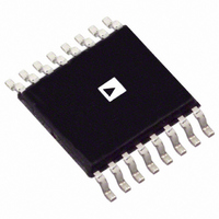
IC AMP VGA DIFF LN 16TSSOP
Manufacturer
Analog Devices Inc
Type
Var Gain Ampr
Datasheet
1.AD8370AREZ-RL7.pdf
(28 pages)
Specifications of AD8370AREZ
Amplifier Type
Variable Gain
Number Of Circuits
1
Output Type
Differential
Slew Rate
5750 V/ns
-3db Bandwidth
750MHz
Current - Input Bias
400pA
Current - Supply
79mA
Voltage - Supply, Single/dual (±)
3 V ~ 5.5 V
Operating Temperature
-40°C ~ 85°C
Mounting Type
Surface Mount
Package / Case
16-TSSOP Exposed Pad, 16-eTSSOP, 16-HTSSOP
No. Of Amplifiers
1
Bandwidth
750MHz
No. Of Channels
1
Supply Voltage Range
3V To 5.5V
Amplifier Case Style
TSSOP
No. Of Pins
16
Operating Temperature Range
-40°C To +85°C
Number Of Channels
1
Number Of Elements
2
Power Supply Requirement
Single
Common Mode Rejection Ratio
77dB
Voltage Gain Db
34dB
Input Resistance
0.0002@5VMohm
Input Bias Current
0.9@5VnA
Single Supply Voltage (typ)
5V
Dual Supply Voltage (typ)
Not RequiredV
Power Dissipation
575mW
Rail/rail I/o Type
No
Single Supply Voltage (min)
3V
Single Supply Voltage (max)
5.5V
Dual Supply Voltage (min)
Not RequiredV
Dual Supply Voltage (max)
Not RequiredV
Operating Temp Range
-40C to 85C
Operating Temperature Classification
Industrial
Mounting
Surface Mount
Pin Count
16
Package Type
TSSOP EP
Lead Free Status / RoHS Status
Lead free / RoHS Compliant
Current - Output / Channel
-
Gain Bandwidth Product
-
Voltage - Input Offset
-
Lead Free Status / Rohs Status
Compliant
Available stocks
Company
Part Number
Manufacturer
Quantity
Price
Company:

Part Number:
AD8370AREZ
Manufacturer:
ADI
Quantity:
1 636
Part Number:
AD8370AREZ
Manufacturer:
ADI/亚德诺
Quantity:
20 000
Part Number:
AD8370AREZ-REEL7
Manufacturer:
ADI/亚德诺
Quantity:
20 000
Company:
Part Number:
AD8370AREZ-RL7
Manufacturer:
AD
Quantity:
735
Part Number:
AD8370AREZ-RL7
Manufacturer:
ADI/亚德诺
Quantity:
20 000


AD8370
PIN CONFIGURATION AND FUNCTION DESCRIPTIONS
Table 3. Pin Function Descriptions
Pin No.
1
2, 15, PADDLE
3
4
5
6, 11
7, 10
8
9
12
13
14
16
Mnemonic
INHI
ICOM
VCCI
PWUP
VOCM
VCCO
OCOM
OPHI
OPLO
LTCH
CLCK
DATA
INLO
Description
Balanced Differential Input. Internally biased.
Input Common. Connect to a low impedance ground. This node is also connected to the exposed pad
on the bottom of the device.
Input Positive Supply. 3.0 V to 5.5 V. Should be properly bypassed.
Power Enable Pin. Device is operational when PWUP is pulled high.
Common-Mode Output Voltage Pin. The midsupply ((V
to this pin for external bypassing for additional common-mode supply decoupling. This can be achieved
with a bypass capacitor to ground. This pin is an output only and is not to be driven externally.
Output Positive Supply. 3.0 V to 5.5 V. Should be properly bypassed.
Output Common. Connect to a low impedance ground.
Balanced Differential Output. Biased to midsupply.
Balanced Differential Output. Biased to midsupply.
Serial Data Latch Pin. Serial data is clocked into the shift register via the DATA pin when LTCH is low. Data
in shift register is latched on the next high-going edge.
Serial Clock Input Pin.
Serial Data Input Pin.
Balanced Differential Input. Internally biased.
OCOM
PWUP
VOCM
VCCO
ICOM
OPHI
VCCI
INHI
Figure 3.16-Lead TSSOP
1
2
3
4
5
6
7
8
Rev. A | Page 6 of 28
(Not to Scale)
AD8370
TOP VIEW
16
15
14
13
12
11
10
9
INLO
ICOM
DATA
CLCK
LTCH
VCCO
OCOM
OPLO
VCCO
− V
OCOM
)/2) common-mode voltage is delivered
Related parts for AD8370AREZ
Image
Part Number
Description
Manufacturer
Datasheet
Request
R

Part Number:
Description:
±1.7g Dual-Axis IMEMS Accelerometer Evaluation Board
Manufacturer:
Analog Devices Inc
Datasheet:

Part Number:
Description:
Inertial Sensor Evaluation System
Manufacturer:
Analog Devices Inc
Datasheet:
Part Number:
Description:
Manufacturer:
Analog Devices Inc
Datasheet:
Part Number:
Description:
Manufacturer:
Analog Devices Inc
Datasheet:
Part Number:
Description:
Manufacturer:
Analog Devices Inc
Datasheet:
Part Number:
Description:
Manufacturer:
Analog Devices Inc
Datasheet:
Part Number:
Description:
Manufacturer:
Analog Devices Inc
Datasheet:
Part Number:
Description:
Manufacturer:
Analog Devices Inc
Datasheet:
Part Number:
Description:
Manufacturer:
Analog Devices Inc
Datasheet:
Part Number:
Description:
Manufacturer:
Analog Devices Inc
Datasheet:
Part Number:
Description:
Manufacturer:
Analog Devices Inc
Datasheet:
Part Number:
Description:
Manufacturer:
Analog Devices Inc
Datasheet:
Part Number:
Description:
Manufacturer:
Analog Devices Inc
Datasheet: