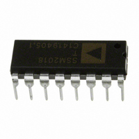
SSM2018TPZ Analog Devices Inc, SSM2018TPZ Datasheet - Page 11

SSM2018TPZ
Manufacturer Part Number
SSM2018TPZ
Description
IC AMP AUDIO MONO CLASS AB 16DIP
Manufacturer
Analog Devices Inc
Datasheet
1.SSM2018PZ.pdf
(16 pages)
Specifications of SSM2018TPZ
Amplifier Type
Audio
Number Of Circuits
1
Slew Rate
5 V/µs
Gain Bandwidth Product
14MHz
Current - Input Bias
250nA
Voltage - Input Offset
1000µV
Current - Supply
11mA
Voltage - Supply, Single/dual (±)
10 V ~ 36 V, ±5 V ~ 18 V
Operating Temperature
-40°C ~ 85°C
Mounting Type
Through Hole
Package / Case
16-DIP (0.300", 7.62mm)
Amplifier Class
AB
No. Of Channels
1
Supply Voltage Range
± 5V To ± 18V
Load Impedance
100kohm
Operating Temperature Range
-40°C To +85°C
Amplifier Case Style
DIP
No. Of Pins
16
Rohs Compliant
Yes
Lead Free Status / RoHS Status
Lead free / RoHS Compliant
Output Type
-
Current - Output / Channel
-
-3db Bandwidth
-
Available stocks
Company
Part Number
Manufacturer
Quantity
Price
Company:
Part Number:
SSM2018TPZ
Manufacturer:
MICREL
Quantity:
12 500
REV. B
As explained above, the gain constant has a –3500 ppm/∞C that
is due to its reciprocal dependence on absolute temperature.
This will cause the gain to vary by 7 dB over the temperature
range from –40∞C to +85∞C when the nominal gain at room
temperature is set to 20 dB. Of course, the gain change is quite
small if the temperature range of operation is restricted. Never-
theless, the TC of the gain constant is easily compensated by
buffering the control voltage to the VCA with a circuit having a
3500 ppm/∞C temperature coefficient. Figure 4 shows a simple
solution to the problem using an op amp with a PT146 tem-
perature compensating resistor from the Precision Resistor
Company. Note that this circuit is inverting, which will change
the gain constant to a positive quantity. Any other circuit that
provides the necessary positive TC will work.
Digital Control of the Gain
A common method of controlling the gain of a VCA is to use a
digital-to-analog converter to set the control voltage. Figure 5
shows a 12-bit DAC, the DAC8512, controlling the SSM2018T.
The DAC8512 is a complete 12-bit converter in an 8-pin pack-
age. It includes an on-board reference and an output amplifier
to produce an output voltage from 0 V to 4.095 V, which is 1
mV/bit. Since the voltage is always positive, this circuit only
provides attenuation. The resistor divider on the output of the
DAC8512 is set to scale the output voltage so that full scale
produces 80 dB of attenuation. The resistor divider can be
adjusted to provide other attenuation ranges. If a parallel inter-
face is needed, then the DAC8562 may be used or, for a dual
DAC, the AD8582.
Supply Considerations and Single Supply Operation
The SSM2018T has a wide operating supply range. Many of the
graphs in this data sheet show the performance of the part from
± 5 V to ± 18 V. These graphs offer typical performance specifi-
cations and are a good indication of the parts’ capabilities. The
minimum operating supply voltage is ± 4.5 V. Below this voltage,
the parts are inoperable. Thus, to account for supply variations,
the recommended minimum supply is ± 5 V.
+15V
V
IN
Figure 5. 12-Bit DAC Controls the VCA Gain
0.1 F
18k
SCLK
CLR
SDI
CS
LD
47pF
NC
NC
DAC8512
+5V
SSM2018T
0.1 F
18k
50pF
NC = NO CONNECT
825
R6
NC
NC
1k
R7
0V
150k
V
C
0.1 F
C
1 F
V
+15V
–15V
CON
+2.24V
OUT
–11–
For simplicity the circuits in the data sheet do not show supply
decoupling; however, to ensure best performance, each supply pin
should be decoupled with a 0.1 mF ceramic (or other low resistance
and inductance type) capacitor as close to the package as possible.
This minimizes the chance of supply noise feeding through the part
causing excessive noise in the audio frequency range.
The SSM2018T can be operated in single supply mode as long
as the circuit is properly biased. Figure 6 shows the proper con-
figuration, which includes an amplifier to create a false ground
node midway between the supplies. A high quality, wide band-
width audio amplifier, such as the OP176 or AD797, should
be used to ensure a very low impedance ground over the full
audio frequency range. The minimum operating supply for the
SSM2018T is ± 5 V, which gives a minimum single supply of
+10 V and ground. The performance of the circuit with +10 V
is identical to graphs that show operation of the SSM2018T
with ± 5 V supplies.
Operational Voltage Controlled Element
The SSM2018T has considerable flexibility beyond the basic VCA
circuit utilized throughout this data sheet. The name “Operational
Voltage Controlled Element” comes from the fact that the part
behaves much like an operational amplifier with a second voltage
controlled output. The symbol for the OVCE connected as a unity
gain follower/VCA is shown in Figure 7. The voltage output labeled
V
feedback. The V
upon the control voltage.
Because the OVCE works just like an op amp, the feedback could
as easily have included resistors to add gain, or a filter network
to add frequency shaping. The full circuit for the OVCE is shown
in Figure 8. Notice that the amplifier whose output (Pin 16) was
originally connected to V
As mentioned before, because the SSM2018T is trimmed for
the basic VCA configuration, potentiometers are needed for the
OVCE configuration to ensure the best THD and control
feedthrough performance.
V
V
1–G
IN+
IN–
is fed back to the inverting input just as it is for an op amp’s
1 F
Figure 6. Single Supply Operation of SSM2018T
1 F 18k
18k
V+
100k
100k
47pF
G
V+
output is amplified or attenuated depending
SSM2018T
10 F
50pF
18k
MINUS
OP176
V+
is now the output for feedback.
1 F
R
B
V
SSM2018T
OUT
V+
1k
3k
V
CONTROL


