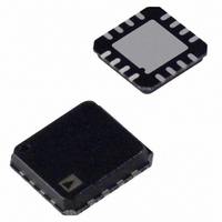
ADA4932-1YCPZ-R2 Analog Devices Inc, ADA4932-1YCPZ-R2 Datasheet - Page 5

ADA4932-1YCPZ-R2
Manufacturer Part Number
ADA4932-1YCPZ-R2
Description
IC AMP DIFF LP 80MA 16LFCSP
Manufacturer
Analog Devices Inc
Datasheet
1.ADA4932-1YCPZ-R7.pdf
(28 pages)
Specifications of ADA4932-1YCPZ-R2
Design Resources
Single-Ended-to-Differential High Speed Drive Circuit for 16-Bit, 10 MSPS AD7626 ADC (CN0105)
Amplifier Type
Differential
Number Of Circuits
1
Output Type
Differential
Slew Rate
2800 V/µs
-3db Bandwidth
560MHz
Current - Input Bias
2.5µA
Voltage - Input Offset
500µV
Current - Supply
9.6mA
Current - Output / Channel
80mA
Voltage - Supply, Single/dual (±)
3 V ~ 11 V, ±1.5 V ~ 5.5 V
Operating Temperature
-40°C ~ 105°C
Mounting Type
Surface Mount
Package / Case
16-LFCSP
No. Of Amplifiers
1
Input Offset Voltage
2.2mV
Bandwidth
560MHz
Supply Voltage Range
3V To 11V
Supply Current
9.6mA
Amplifier Case Style
LFCSP
No. Of Pins
16
Rohs Compliant
Yes
Lead Free Status / RoHS Status
Lead free / RoHS Compliant
Gain Bandwidth Product
-
5 V OPERATION
T
All specifications refer to single-ended input and differential outputs, unless otherwise noted. Refer to Figure 55 for signal definitions.
±D
Table 4.
Parameter
DYNAMIC PERFORMANCE
NOISE/HARMONIC PERFORMANCE
INPUT CHARACTERISTICS
OUTPUT CHARACTERISTICS
A
Second Harmonic
Third Harmonic
IMD
Voltage Noise (RTI)
Input Current Noise
Crosstalk
Offset Voltage
Input Bias Current
Input Offset Current
Input Resistance
Input Capacitance
Input Common-Mode Voltage Range
CMRR
Open-Loop Gain
Output Voltage Swing
Linear Output Current
Output Balance Error
−3 dB Small Signal Bandwidth
−3 dB Large Signal Bandwidth
Bandwidth for 0.1 dB Flatness
Slew Rate
Settling Time to 0.1%
Overdrive Recovery Time
= 25°C, +V
IN
to V
OUT, dm
S
= 5 V, −V
Performance
S
= 0 V, V
OCM
= 2.5 V, R
Conditions
V
V
V
V
V
V
V
V
V
See Figure 54 for distortion test circuit
V
V
V
V
V
V
V
V
f
f = 1 MHz
f = 1 MHz
f = 10 MHz, ADA4932-2
V
T
T
Differential
Common mode
∆V
Maximum ∆V
R
200 kHz, R
∆V
see Figure 53 for output balance test circuit
1
MIN
MIN
OUT, dm
OUT, dm
OUT, dm
OUT, dm
OUT, dm
OUT, dm
OUT, dm
OUT, dm
IN
OUT, dm
OUT, dm
OUT, dm
OUT, dm
OUT, dm
OUT, dm
OUT, dm
OUT, dm
+DIN
F
= 30 MHz, f
= R
OUT, dm
OUT, cm
= 0 V to 2.5 V ramp, G = 2
to T
to T
= V
G
F
= 0.1 V p-p
= 0.1 V p-p, R
= 2.0 V p-p
= 2.0 V p-p, R
= 2.0 V p-p, ADA4932-1, R
= 2.0 V p-p, ADA4932-2, R
= 2 V p-p, 25% to 75%
= 2 V step
= 2 V p-p, 1 MHz
= 2 V p-p, 10 MHz
= 2 V p-p, 20 MHz
= 2 V p-p, 50 MHz
= 2 V p-p, 1 MHz
= 2 V p-p, 10 MHz
= 2 V p-p, 20 MHz
= 2 V p-p, 50 MHz
= 10 kΩ, R
= 499 Ω, R
/∆V
MAX
MAX
/∆V
−DIN
L, dm
variation
variation
OUT, dm
IN, cm
= V
2
OUT
= 10 Ω, SFDR = 67 dB
= 30.1 MHz, V
OCM
, ∆V
, single-ended output,
, ∆V
L
= 1 kΩ
G
= 2.5 V
IN, cm
Rev. A | Page 5 of 28
F
F
OUT, dm
= 499 Ω, R
= R
= R
= ±1 V
G
G
= 205 Ω
= 205 Ω
= 1 V p-p, 1 MHz,
OUT, dm
T
L
L
= 53.6 Ω (when used), R
= 2 V p-p
= 200 Ω
= 200 Ω
Min
−2.2
−5.3
−0.25
64
−V
+V
S
S
+ 1.15 to
− 1.15
L, dm
ADA4932-1/ADA4932-2
= 1 kΩ, unless otherwise noted.
Typ
560
990
315
320
120
200
2200
10
20
−110
−100
−90
−72
−120
−100
−87
−70
−91
3.6
1.0
−100
±0.5
−3.7
−3.0
−9.5
±0.025
11
16
0.5
−V
+V
−100
66
−V
+V
53
−64
S
S
S
S
+ 0.2 to
− 1.8
+ 1.02 to
− 1.02
Max
+2.2
−0.23
+0.25
−87
−60
Unit
MHz
MHz
MHz
MHz
MHz
MHz
V/μs
ns
ns
dBc
dBc
dBc
dBc
dBc
dBc
dBc
dBc
dBc
nV/√Hz
pA/√Hz
dB
mV
μV/°C
μA
nA/°C
μA
MΩ
MΩ
pF
V
dB
dB
V
mA rms
dB


